Visible to Intel only — GUID: vom1698164070268
Ixiasoft
Visible to Intel only — GUID: vom1698164070268
Ixiasoft
3.3. Configure and Generate the AXI Streaming Intel® FPGA IP for PCI Express*
You can generate the AXI Streaming Intel® FPGA IP for PCI Express* as per the following process:
| AXI Streaming Intel® FPGA IP for PCI Express* in | Description |
|---|---|
| Standalone mode | Refer to the steps listed below to generate the IP in standalone mode. |
| Design example | Refer to the steps listed below to generate the IP as part of the design example. |
| Intel Open FPGA Stack (OFS) reference design | You can use the Intel pre-designed and verified system level shell designs (e.g., Open FPGA Stack (OFS)) with the IP and other Intel FPGA IPs like DMA, etc., and software stack to run example workloads.
Note: For examples on connecting the various interfaces of the AXI Streaming Intel® FPGA IP for PCI Express* , you can access the following design repository: Open FPGA Stack Overview.
|
Following is the procedure to generate the AXI Streaming Intel® FPGA IP for PCI Express* and bring up a PCI Express* link using Quartus® Prime Pro Edition software in standalone mode.
- Use the Quartus® Prime Pro Edition software to create a Quartus Project and select the device. Currently, the AXI Streaming Intel® FPGA IP for PCI Express* is only supported on Agilex™ 7 devices with P-Tile (e.g., AGFB014R24B2E2V), F-Tile (e.g. AGIB027R29A1E2VR2), and R-Tile (AGIB027R29A1E2VR3).
- Use the following steps to specify IP core options and parameters:
- In the Quartus® Prime Pro Edition software, create a new project (File > New Project Wizard).
- Specify the Directory, Name, and Top-Level Entity.
- For Project Type, accept the default value, Empty project. Click Next.
- For Add Files click Next.
- For Family, Device & Board Settings under Family, select Agilex™ 7 .
- Select the Target Device for your design.
- Click Finish.
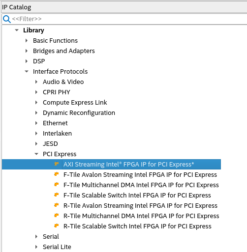
- In the IP Catalog, locate and add the AXI Streaming Intel® FPGA IP for PCI Express* . This IP is available under the PCI Express IPs.

- In the New IP Variant dialogue box, specify a name for your IP. The Parameter Editor saves the IP variation settings in a file named <your_ip>.ip
- Click Create. The Parameter Editor appears.
- Specify the parameters for your IP core variation. Refer to Parameter Editor Parameters for information about specific IP core parameters.
- Generate the IP:
- Generation dialogue box appears from the previous step. This allows you to generate the IP in the stand-alone mode.
- Specify output file generation options, and then click Generate. The IP variation files are generated according to your specifications.
- Click Close. The Parameter Editor adds the top-level.ip file to the current project automatically. If you are prompted to manually add the .ip file to the project, click Project > Add/Remove Files in Project to add the file.
- On the PCIe Interfaces and PCIe Interfaces Settings tabs, specify the parameters for your IP variation.
If you want to generate the SR-IOV design example, perform the following steps to enable SR-IOV:
- On the PCIe Interfaces Settings tab, set the PCIe Hard IP Mode parameter to the SR-IOV-supported Tile and configuration.
- On the PCIe Interfaces Ports Settings tab, navigate to PCIe0 PCI Express/PCI Capabilities > PCIe0 Device > PCIe0 Multifunction and SR-IOV System Settings and:
- Check the Enable Multiple Physical Functions parameter.
- Set the Total Physical Functions (PFs) parameter to 2.
- Check the Enable SR-IOV Support parameter.
- Set the Total Virtual Functions of Physical Function 0 (PF0 VFs) parameter to 16.
- Set the Total Virtual Functions of Physical Function 1 (PF1 VFs) parameter to 16.
- On the PCIe0 Settings tab, navigate to PCIe0 Base Address Registers > PCIe0 PF0 BAR Configuration > PCIe0 PF0 BAR and:
- Set the BAR0 Type parameter to 64-bit prefetchable memory, 64-bit non-prefetchable memory, or 32-bit non-prefetchable memory.
- Set the BAR0 Size parameter to any value other than N/A.
- Repeat steps i and ii for PCIe0 PF0 BAR above in the PCIe0 PF0 VF BAR section.
- On the PCIe0 Settings tab, navigate to PCIe0 Base Address Registers > PCIe0 PF1 BAR Configuration > PCIe0 PF1 BAR and:
- Set the BAR0 Type parameter to 64-bit prefetchable memory, 64-bit non-prefetchable memory, or 32-bit non-prefetchable memory.
- Set the BAR0 Size parameter to any value other than N/A.
- Repeat steps i and ii for PCIe0 PF1 BAR above in the PCIe0 PF1 VF BAR section.
- On the PCIe0 Settings tab, navigate to PCIe0 PCI Express/PCI Capabilities > PCIe0 MSI-X > PCIe0 PF MSI-X > PCIe0 PF0 MSI-X and check the Enable MSI-X parameter.
- On the PCIe0 Settings tab, navigate to PCIe0 PCI Express/PCI Capabilities > PCIe0 MSI-X > PCIe0 PF MSI-X > PCIe0 PF1 MSI-X and check the Enable MSI-X parameter.
- On the PCIe0 Settings tab, navigate to PCIe0 Device Identification Registers and set the following parameters for the PCIe0 PF0 IDs and PCIe0 PF1 IDs:
- Vendor ID: 0x00001172
- Device ID: 0x00000000
- Revision ID: 0x00000001
- Class Code: 0x00ff0000
- Subsystem Vendor ID: 0x00001172
- Subsystem Device ID: 0x00000000
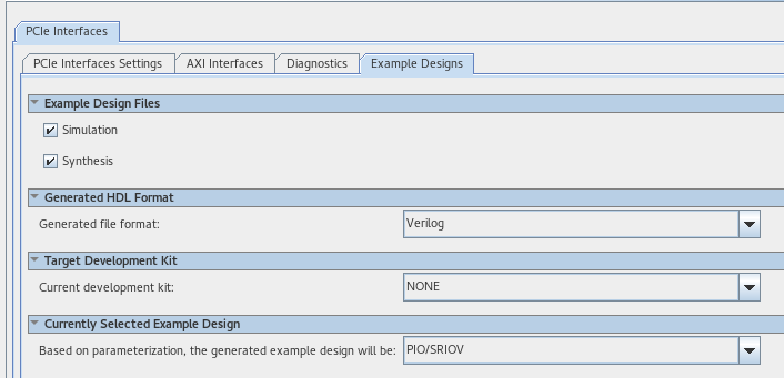
- To generate the design example, go to the Example Designs tab. Make the following selections:
- For Example Design Files, turn on the Simulation and Synthesis options. If you do not need these simulation or synthesis files, leaving the corresponding option(s) turned off significantly reduces the design example generation time.
- For General HDL Format, only Verilog is available in the current release.
- For Target Development Kit, select the FPGA development kit corresponding to the device being used in the project.

- For Currently Selected Example Design, select the PIO. SR-IOV, or Performance design example.
- Select Generate Example Design to create a design example that you can simulate and download to hardware. If you select one of the development boards, the device on that board overwrites the device previously selected in the Intel Quartus Prime project if the devices are different. When the prompt asks you to specify the directory for your design example, you can accept the default directory, ./<ip__example_design>, or choose another directory.
- Close the window when the design example generation is done. You may save your .ip file when prompted, but it is not required to be able to use the design example.
- Open the design example project by navigating to <project_dir>/<ip_example_design>/ and opening the file pcie_ed.qpf.
- Compile the design example project to generate the .sof file for the complete design example. This file is what you download to a board to perform hardware verification. For details on how to compile the design, refer to Compiling the Design Example.
- Close your design example project. Note that you cannot change the PCIe pin allocations in the Intel Quartus Prime project. However, to ease PCB routing, you can take advantage of the lane reversal and polarity inversion features supported by this IP.
- Only simulation support is available.
- Only Gen5 x16 (R-Tile) and Gen4 x16 (P-Tile) are available.