Visible to Intel only — GUID: khg1708015126729
Ixiasoft
Visible to Intel only — GUID: khg1708015126729
Ixiasoft
9.3.1. LPDDR5 PCB Stackup and Design Considerations
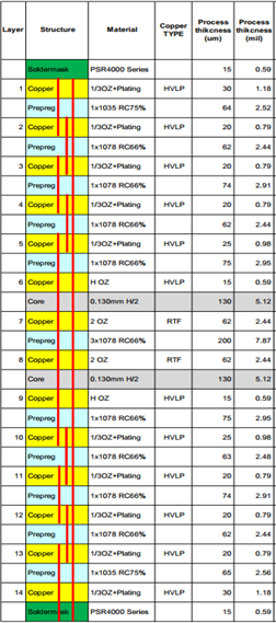
The following figures show an example of a PCB stackup with 14 layers that has been used on PCB design for an Intel platform board. You may use other stackups (thin such as PCIE board or thick board) if you meet the recommendations in this guideline.
The figure below shows a 14L thin board, high performance Type-IV PCB with micro vias, stacked vias, buried vias and through vias.

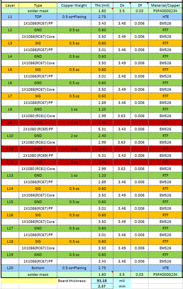
The figure below shows a 20L thick Type-III Board stack-up (high performance with PTH with/without backdrill example used at Altera platform boards and development kits.

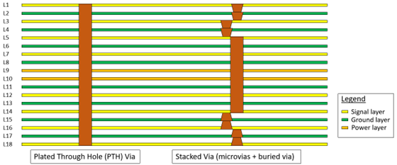
A type-IV PCB is a precise and high-quality PCB. This type-IV PCB utilizes not only PTH vias to connect from top to bottom layers, but also stacked vias, micro vias and buried vias to connect between layers. For example, a full-height stacked via of a 14-layer PCB is made up of a combination of dual-stacked micro vias and buried vias. depicts a cross-sectional comparison of a PTH and a stacked via.
A type-III PCB board with PTH vias, which is used to implement DDR4 designs and can also be used for LPDDR5 designs.
