Visible to Intel only — GUID: dxp1680406018201
Ixiasoft
1. About the External Memory Interfaces Agilex™ 5 FPGA IP
2. Agilex™ 5 FPGA EMIF IP – Introduction
3. Agilex™ 5 FPGA EMIF IP – Product Architecture
4. Agilex™ 5 FPGA EMIF IP – End-User Signals
5. Agilex™ 5 FPGA EMIF IP – Simulating Memory IP
6. Agilex™ 5 FPGA EMIF IP - DDR4 Support
7. Agilex™ 5 FPGA EMIF IP - DDR5 Support
8. Agilex™ 5 FPGA EMIF IP - LPDDR4 Support
9. Agilex™ 5 FPGA EMIF IP - LPDDR5 Support
10. Agilex™ 5 FPGA EMIF IP – Timing Closure
11. Agilex™ 5 FPGA EMIF IP – Controller Optimization
12. Agilex™ 5 FPGA EMIF IP – Debugging
13. Document Revision History for External Memory Interfaces (EMIF) IP User Guide
3.2.1. Agilex™ 5 EMIF Architecture: I/O Subsystem
3.2.2. Agilex™ 5 EMIF Architecture: I/O SSM
3.2.3. Agilex™ 5 EMIF Architecture: HSIO Bank
3.2.4. Agilex™ 5 EMIF Architecture: I/O Lane
3.2.5. Agilex™ 5 EMIF Architecture: Input DQS Clock Tree
3.2.6. Agilex™ 5 EMIF Architecture: PHY Clock Tree
3.2.7. Agilex™ 5 EMIF Architecture: PLL Reference Clock Networks
3.2.8. Agilex™ 5 EMIF Architecture: Clock Phase Alignment
3.2.9. User Clock in Different Core Access Modes
6.2.3.1. Address and Command Pin Placement for DDR4
6.2.3.2. DDR4 Data Width Mapping
6.2.3.3. General Guidelines
6.2.3.4. x4 DIMM Implementation
6.2.3.5. Specific Pin Connection Requirements
6.2.3.6. Command and Address Signals
6.2.3.7. Clock Signals
6.2.3.8. Data, Data Strobes, DM/DBI, and Optional ECC Signals
6.4.3.1. 1 Rank x 8 Discrete (Memory Down) Topology
6.4.3.2. 1 Rank x 16 Discrete (Memory Down) Topology
6.4.3.3. VREF_CA/RESET Signal Routing Guidelines for 1 Rank x 8 and 1 Rank x 16 Discrete (Memory Down) Topology
6.4.3.4. Skew Matching Guidelines for DDR4 (Memory Down) Discrete Configurations
6.4.3.5. Power Delivery Recommendation for DDR4 Discrete Configurations
6.4.3.6. DDR4 Simulation Strategy
12.1. Interface Configuration Performance Issues
12.2. Functional Issue Evaluation
12.3. Timing Issue Characteristics
12.4. Verifying Memory IP Using the Signal Tap Logic Analyzer
12.5. Debugging with the External Memory Interface Debug Toolkit
12.6. Generating Traffic with the Test Engine IP
12.7. Guidelines for Developing HDL for Traffic Generator
12.8. Guidelines for Traffic Generator Status Check
12.9. Hardware Debugging Guidelines
12.10. Create a Simplified Design that Demonstrates the Same Issue
12.11. Measure Power Distribution Network
12.12. Measure Signal Integrity and Setup and Hold Margin
12.13. Vary Voltage
12.14. Operate at a Lower Speed
12.15. Determine Whether the Issue Exists in Previous Versions of Software
12.16. Determine Whether the Issue Exists in the Current Version of Software
12.17. Try A Different PCB
12.18. Try Other Configurations
12.19. Debugging Checklist
12.20. Categorizing Hardware Issues
12.21. Signal Integrity Issues
12.22. Characteristics of Signal Integrity Issues
12.23. Evaluating Signal Integrity Issues
12.24. Skew
12.25. Crosstalk
12.26. Power System
12.27. Clock Signals
12.28. Address and Command Signals
12.29. Read Data Valid Window and Eye Diagram
12.30. Write Data Valid Window and Eye Diagram
12.31. Hardware and Calibration Issues
12.32. Memory Timing Parameter Evaluation
12.33. Verify that the Board Has the Correct Memory Component or DIMM Installed
Visible to Intel only — GUID: dxp1680406018201
Ixiasoft
8.2.1.2. LPDDR4 Component Options
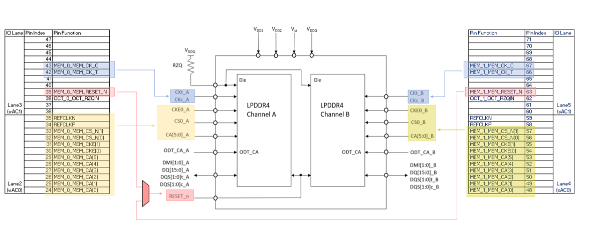
The table and figure below illustrate the pin placement and routing recommendation for a single 32-bit channel, and two 16-bit channels, respectively.
Note: Always consult your memory vendor’s data sheet to verify pin placement and routing plans.
| Pins | 1 CH x32 | 2 CH x16 | |
|---|---|---|---|
| Data | DQ[15:0]_A DQ[15:0]_B |
DQ[15:0]_A |
DQ[15:0]_B |
| Data mask | DMI[1:0]_A DMI[1:0]_B |
DMI[1:0]_A |
DMI[1:0]_B |
| Data strobe | DQS[1:0]_t_A DQS[1:0]_c_A DQS[1:0]_t_B DQS[1:0]_t_B |
DQS[1:0]_t_A DQS[1:0]_c_A |
DQS[1:0]_t_B DQS[1:0]_c_B |
| Address/Command | CA[5:0]_A CS0_A CA[5:0]_B CS0_B |
CA[5:0]_A CS0_A |
CA[5:0]_B CS0_B |
| Clock | CK_t_A CK_c_A CK_t_B CK_c_B |
CK_t_A CK_c_A |
CK_t_B CK_c_B |
| Clock Enable | CKE_A CKE_B |
CKE_A | CKE_B |
| Reset | RESET_n |
RESET_n (Resistor jumper to select from mem_0 or mem_1.) |
|
Figure 31. Single-Channel x32 LPDDR4, Single Rank
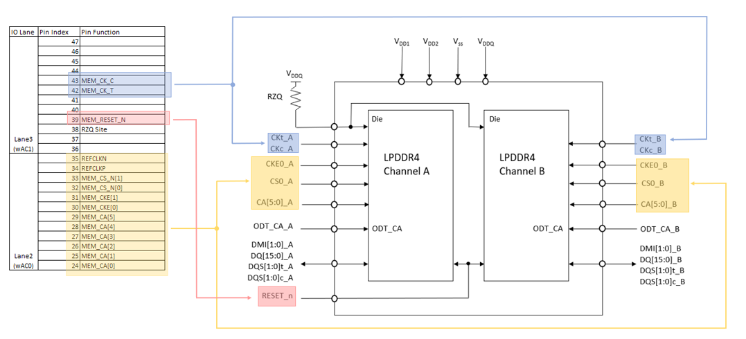
Figure 32. Dual-Channel x16 LPDDR4, Single Rank