Visible to Intel only — GUID: joe1707953504069
Ixiasoft
Visible to Intel only — GUID: joe1707953504069
Ixiasoft
6.4.2. DDR4 General Design Considerations
General DDR Signal Routing Guideline on PCB
Altera recommends to route all data signals within a specific group on the same layer.
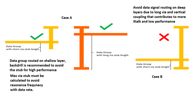
The figure below illustrates a routing example for a type-III PCB board for a DDR4 design. Data Group signals such as DQ, DM and DQS signals should be routed on shallow layers as stripline with the least Z-height via transition to avoid vertical crosstalk to achieve high performance.
For example, the recommended routing layers for data group on a 20-layers board and using PTH via will be on the top half of the PCB such as L3, L5 and L7. Other signals such as CA, CTRL and clock signals can be routed with longer Z-height via transition on the bottom half of the PCB such as L14, L16 and L18.
Minimal stub effect or back drill is recommended, but not mandatory, to avoid high reflection for maximum data rate performance. Long via stubs will affect the ISI of channel but the impact of ISI is less than impact of crosstalk for the max data rate performance.

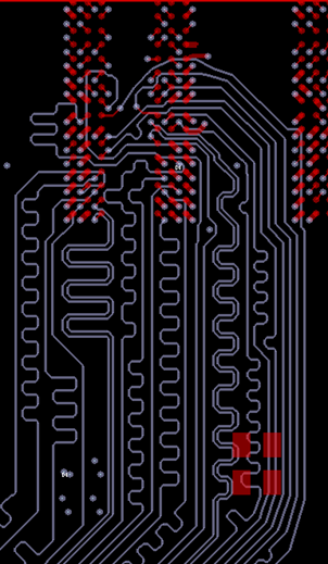
To minimize crosstalk horizontally between signals on the same layer, PCB designers must maintain adequate signal trace-to-trace (edge to edge) space, with a minimum spacing of 3xH separation distance, where H is the dielectric thickness to the closest reference plane as illustrated in the figure below.

DDR FPGA Break Out Routing
Agilex™ 5 devices come with various pitch sizes for different FPGA pins. The GPIO pin pitch is very small, the device BGA pad stack is also very small, therefore, it is highly recommended to use a dog bone configuration for inner GPIO pins fanout along with stripline routing; however, for the GPIO pins on the edge of device, Altera recommends to use microstrip routing. Both microstrip and stripline routing guidelines are presented in this document for all supported EMIF interfaces and topologies.
DDR Differential Signals Routing
DQS and CLK signals in the DDR interface are differential signals and must be routed on PCB as differential signals unless there is a limitation for PCB routing such as having a very small pitch at DRAM area.
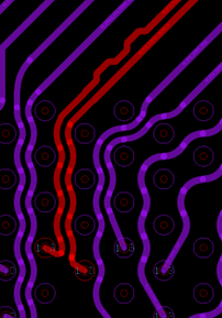
Intel recommends a symmetrical fan-out routing at the FPGA pin field. Non-symmetrical routing for differential signals will cause shifting on common-mode voltage and contributes to reduced timing margins at the receiver. The following figures show the recommended differential routing at the FPGA pin field for DQS/CLK signals.
The figure below shows the symmetrical routing of differential signals (DQS/CLK) at FPGA pin field along with length/skew matching between P/N lanes right after FPGA device edge.

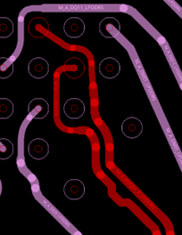
The figure below shows the single-ended routing for differential signals (DQS/CLK) at DRAM pin field if the pitch is very small along with skew matching right at edge of DRAM pin field.

Altera recommends to implement length/skew matching for differential signals (if there is) right after FPGA device to avoid additional shifting on differential signals common mode voltage.
In case of having limitation for implementing symmetrical routing at DRAM pin field for differential signals due to very small pitch, Altera recommends to route the differential signals as single-ended signals within the DRAM pin field, ensuring to keep the same impedance while changing from differential to single-ended configuration. Designers must also keep the same length of routing for each P and N single-ended lane within the DRAM pin field. The skew matching between P/N lanes must be applied before reaching the DRAM pin field.
Ground Plane and Return Path
A continuous and solid ground reference plane is crucial for data lines to ensure good signal integrity performance. Low impedance ground return path from the FPGA to DRAM devices should be provisioned. In addition, it is desirable to keep ground stitching vias within 80 mils from signal transition for better return path on signal via and better signal integrity performance.
DRAM Break Out in Layout Guideline
For discrete DRAM components on PCB, you can either use the dog-bone or via in pad at DRAM for the signal transition from inner layer to DRAM. If dog-bone via transition is used, it is recommended to separate them with larger pitch to avoid crosstalk between signal vias.
