Visible to Intel only — GUID: gcb1715691609247
Ixiasoft
1. About the External Memory Interfaces Agilex™ 5 FPGA IP
2. Agilex™ 5 FPGA EMIF IP – Introduction
3. Agilex™ 5 FPGA EMIF IP – Product Architecture
4. Agilex™ 5 FPGA EMIF IP – End-User Signals
5. Agilex™ 5 FPGA EMIF IP – Simulating Memory IP
6. Agilex™ 5 FPGA EMIF IP - DDR4 Support
7. Agilex™ 5 FPGA EMIF IP - DDR5 Support
8. Agilex™ 5 FPGA EMIF IP - LPDDR4 Support
9. Agilex™ 5 FPGA EMIF IP - LPDDR5 Support
10. Agilex™ 5 FPGA EMIF IP – Timing Closure
11. Agilex™ 5 FPGA EMIF IP – Controller Optimization
12. Agilex™ 5 FPGA EMIF IP – Debugging
13. Document Revision History for External Memory Interfaces (EMIF) IP User Guide
3.2.1. Agilex™ 5 EMIF Architecture: I/O Subsystem
3.2.2. Agilex™ 5 EMIF Architecture: I/O SSM
3.2.3. Agilex™ 5 EMIF Architecture: HSIO Bank
3.2.4. Agilex™ 5 EMIF Architecture: I/O Lane
3.2.5. Agilex™ 5 EMIF Architecture: Input DQS Clock Tree
3.2.6. Agilex™ 5 EMIF Architecture: PHY Clock Tree
3.2.7. Agilex™ 5 EMIF Architecture: PLL Reference Clock Networks
3.2.8. Agilex™ 5 EMIF Architecture: Clock Phase Alignment
3.2.9. User Clock in Different Core Access Modes
6.2.3.1. Address and Command Pin Placement for DDR4
6.2.3.2. DDR4 Data Width Mapping
6.2.3.3. General Guidelines
6.2.3.4. x4 DIMM Implementation
6.2.3.5. Specific Pin Connection Requirements
6.2.3.6. Command and Address Signals
6.2.3.7. Clock Signals
6.2.3.8. Data, Data Strobes, DM/DBI, and Optional ECC Signals
6.4.3.1. 1 Rank x 8 Discrete (Memory Down) Topology
6.4.3.2. 1 Rank x 16 Discrete (Memory Down) Topology
6.4.3.3. VREF_CA/RESET Signal Routing Guidelines for 1 Rank x 8 and 1 Rank x 16 Discrete (Memory Down) Topology
6.4.3.4. Skew Matching Guidelines for DDR4 (Memory Down) Discrete Configurations
6.4.3.5. Power Delivery Recommendation for DDR4 Discrete Configurations
6.4.3.6. DDR4 Simulation Strategy
12.1. Interface Configuration Performance Issues
12.2. Functional Issue Evaluation
12.3. Timing Issue Characteristics
12.4. Verifying Memory IP Using the Signal Tap Logic Analyzer
12.5. Debugging with the External Memory Interface Debug Toolkit
12.6. Generating Traffic with the Test Engine IP
12.7. Guidelines for Developing HDL for Traffic Generator
12.8. Guidelines for Traffic Generator Status Check
12.9. Hardware Debugging Guidelines
12.10. Create a Simplified Design that Demonstrates the Same Issue
12.11. Measure Power Distribution Network
12.12. Measure Signal Integrity and Setup and Hold Margin
12.13. Vary Voltage
12.14. Operate at a Lower Speed
12.15. Determine Whether the Issue Exists in Previous Versions of Software
12.16. Determine Whether the Issue Exists in the Current Version of Software
12.17. Try A Different PCB
12.18. Try Other Configurations
12.19. Debugging Checklist
12.20. Categorizing Hardware Issues
12.21. Signal Integrity Issues
12.22. Characteristics of Signal Integrity Issues
12.23. Evaluating Signal Integrity Issues
12.24. Skew
12.25. Crosstalk
12.26. Power System
12.27. Clock Signals
12.28. Address and Command Signals
12.29. Read Data Valid Window and Eye Diagram
12.30. Write Data Valid Window and Eye Diagram
12.31. Hardware and Calibration Issues
12.32. Memory Timing Parameter Evaluation
12.33. Verify that the Board Has the Correct Memory Component or DIMM Installed
Visible to Intel only — GUID: gcb1715691609247
Ixiasoft
7.2.3.1. General Guidelines - DDR5
Observe the following general guidelines when placing pins for your Agilex™ 5 external memory interface: .
- Ensure that the pins of a single external memory interface reside on the same edge I/O.
- The address and command pins and their associated clock pins in the address and command bank must follow a fixed pin-out scheme, as defined in the table in the Address and Command Pin Placement for DDR5 topic.
- Not every byte lane can function as an address and command lane or a data lane. The pin assignment must adhere to the DDR5 data width mapping defined in DDR5 Data Width Mapping .
- A byte lane must not be used by both address and command pins and data pins.
- An external memory interface can occupy one or more banks on the same edge. When an interface must occupy multiple banks, ensure that those banks are adjacent to one another.
- If an I/O bank is shared between two interfaces—meaning that two sub-banks belong to two different EMIF interfaces—then both the interfaces must share the same voltage.
- Sharing of I/O lanes within a sub-bank for two different EMIF interfaces is not permitted; I/O lanes within a sub-bank can be assigned to one EMIF interface only.
- Any pin in the same bank that is not used by an external memory interface may not be available for use as a general purpose I/O pin:
- For fabric EMIF, unused pins in an I/O lane assigned to an EMIF interface cannot be used as general-purpose I/O pins. In the same sub-bank, pins in an I/O lane that is not assigned to an EMIF interface, can be used as general-purpose I/O pins.
- For HPS EMIF, unused pins in an I/O lane assigned to an EMIF interface cannot be used as general-purpose I/O pins. In the same bank, pins in an I/O lane that is not assigned to an EMIF interface cannot be used as general-purpose I/O pins either.
- All address and command pins and their associated clock pins (CK_t and CK_c) must reside within a single sub-bank. The sub-bank containing the address and command pins is identified as the address and command sub-bank. Refer to the table in DDR5 Data Width Mapping for the supported address and command and data lane placements for DDR5.
- The address and command pins and their associated clock pins in the address and command bank must follow a fixed pin-out scheme, as defined in the Agilex™ 5 External Memory Interface Pin Information file.
- An external memory interface can occupy one or more banks on the same edge. When an interface must occupy multiple banks, ensure the following:
- That the banks are adjacent to one another.
- That you used only the supported data width mapping as defined in the table in DDR5 Data Width Mapping . Be aware that not every byte lane can be used as an address and command lane or a data lane.
Figure 30. x72 DDR5 Pin Placement using Bank 2A and 2B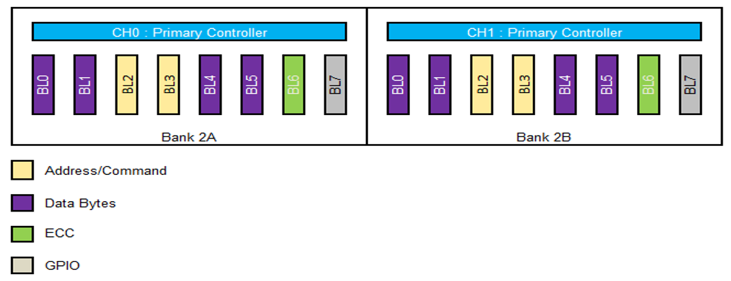
- An unused I/O lane in the address and command sub-bank can serve to implement a data group, such as a x8 DQS group. The data group must be from the same controller as the address and command signals.
- An I/O lane must not be used by both address and command pins and data pins.
- Place read data groups according to the DQS grouping in the pin table and Pin Planner. Read data strobes (such as DQS_t and DQS_c) must reside at physical pins capable of functioning as DQS_t and DQS_c for a specific read data group size. You must place the associated read data pins (DQ), within the same group.
Note: For DDR5 interfaces with x4 components, place DQ pins and DQS entirely in either the upper or lower half of a 12-bit bank sub-group. Consult the pin table for your device to identify the association between DQ pins and DQS pins for x4 mode operation. Additional restrictions apply for x4/x8 DIMM interoperability.
- One of the sub-banks in the device (typically the sub-bank within corner bank 3A) may not be available if you use certain device configuration schemes. For some schemes, there may be an I/O lane available for EMIF data group.
- AVST-8 – This is contained entirely within the SDM, therefore all lanes of sub-bank 3A can be used by the external memory interface.
- AVST-16 – Lanes 4, 5, 6, and 7 are all effectively occupied and are not usable by the external memory interface.
- Two memory interfaces cannot share an I/O 48 sub-bank.