Visible to Intel only — GUID: izp1707936284746
Ixiasoft
Visible to Intel only — GUID: izp1707936284746
Ixiasoft
9.3.3.1. LPDDR5 Discrete Component/Memory Down Topology (Single Rank or Dual-Rank)
There are four DRAM interface signal groupings: data group, command-address group, control group, and clock group. The FPGA to DRAM connection uses point-to-point topology for data group, command-address group, control group, and clock group. The figure below shows the stripline routing topology for inner pins.


The figure below shows the microstrip routing for the edge pins per byte.

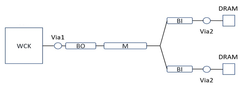
LPDDR5 interfaces do not support traditional dual-directional data-strobe architecture; however, two single-directional data strobes such as Write Clock (WCK) for write operations and an optional Read Clock (RDQS) for read operations are added. The following two figures show the T-Line connection topology for WCK signal and CA, CLK, CTRL signals.
The figure below shows the stripline routing topology for inner pins.

The figure below show the daisy or T-Line connection topology for CA, CLK, and CTRL signals.

The following tables provide a comprehensive routing guideline for each of the LPDDR5 signals based on memory down topology. For example, the trace impedance, the total trace length, the maximum length of the main trace routing can be derived by subtracting break-out and break-in trace segment length routed from total trace length. The signal trace width and minimum spacing and gaps (in mils) from edge to edge of signal traces are based on the default stackup.
The table below shows the stripline routing guidelinefor LPDDR5 memory down topology. The h value in the table represents the minimum substrate height from signal layer to reference layer.

|
The table below shows the microstrip routing for LPDDR5 memory down topology.

|
Reset signal routing design also follows the CMD/ADD/CTRL routing design. Maintain at least 5x h of space between the Reset signal to other signals on the same layer (measured edge to edge). There is no requirement to have skew matching between the Reset and CLK signals.
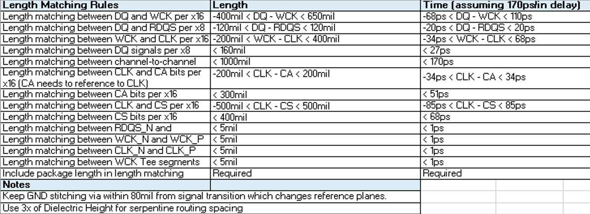
Skew matching for LPDDR5 interfaces consists of both package routing skew and PCB physical routing skew. Skew matching of CA and CTRL with respect to the clock signals must be maintained to ensure signals at the receiver are correctly sampled. In addition, there are skew matching requirements for DQ and DQS within a byte group, DQS and CLK. The table below provides a detailed skew matching guideline to facilitate PCB trace routing efforts.
The length matching criteria in the table below represents a default PCB on an Altera platform board design. Skew matching criteria must be always followed in any other stackups.

|
The LPDDR5 eye margin is sensitive to crosstalk, especially when signals are routed on deep layers in stackup; the deep-layer vertical transition induces greater vertical coupling between signals and hence more crosstalk.
The maximum data rate of LPDDR5 is highly dependent on the DDR memory down configuration and on the type of PCB. For example, with a Type-III PCB, the LPDDR5 interface can run at the maximum data rate for a single-rank x 32 bit LPDDR5 memory down configuration. A reduced data transfer rate is seen whenever 2 x rank LPDDR5 memory down configuration is used.
| Memory | LPDDR5 | |
| Signal group | DQ | |
| Board thickness (mil) | 65mil or 120mil (Routing must be on upper layers) |
65mil or 120mil (Routing must be on upper layers) |
| PCB trace impedance (ohm) | Microstrip line: 45 | Microstrip line: 45 |
| Stripline: 40 | Stripline: 40 | |
| Memory configuration | Memory Down | Memory Down |
| Number of rank | 1 (x16 bits or x32 bits-Double Die) | 2 (x 16 or x 32 bits) |
| Maximum data rate (MT/s) | Refer to Agilex™ 5 data sheet | Refer to Agilex™ 5 data sheet |
| Maximum length total (inch) | Microstrip line: 3.0 | Microstrip line: 3.0 |
| Stripline: 4.0 | Stripline: 4.0 | |