Visible to Intel only — GUID: law1693483195017
Ixiasoft
Visible to Intel only — GUID: law1693483195017
Ixiasoft
8.2. Parameterization Flow
To parameterize the memory subsystem IP, you must first configure the high-level topology by defining the following options:
- The number of memory interfaces, their type, and location.
- The application of the required interfaces.
- The data flow.
After creating and generating the desired high-level topology, you can set more specific parameters and features of each IP within the memory subsystem IP by clicking the Dive Into Packaged Subsystem button.
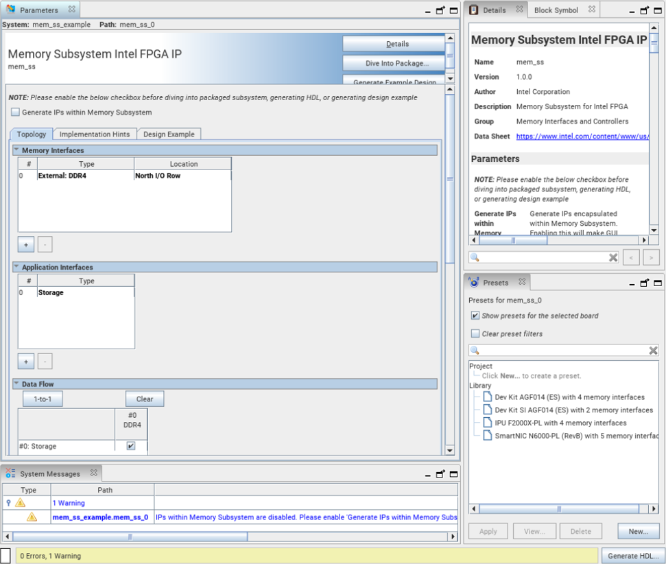
The following figure shows the parameter editor interface. You can define the high-level topology of the memory subsystem IP in this parameter editor. The Details pane at the top-right of the parameter editor displays version information and descriptions of each parameter. The Presets pane at the lower-right displays preset settings for various Intel boards.

The main steps for successfully parameterizing the memory subsystem IP are summarized below:
- Definining the number of memory interfaces, their type, and location.
- Parameterizing the required EMIF, CAM, and MSA IPs.
- Parameterizing the external memory interface (EMIF) IP.
- Parameterizing the memory-specific adapter (MSA).
- Parameterizing the content-addressable memory (CAM) IP.
- Parameterizing the external memory interfaces Intel calibration IP.
The following topics describe each of these main steps in detail. After you have completed these steps, you can then generate an example design that you can compile or simulate, or you can generate the HDL code to create an instance of the IP in your current Intel® Quartus® Prime project