Visible to Intel only — GUID: tuz1665690101120
Ixiasoft
Visible to Intel only — GUID: tuz1665690101120
Ixiasoft
2. Introduction to Memory Subsystem IP
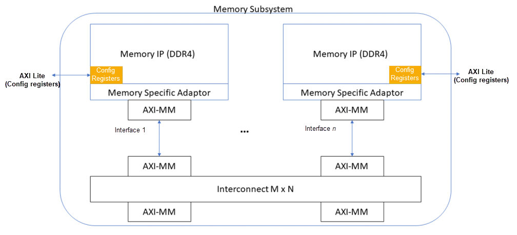
Depending on your requirements, the memory subsystem provides scalable and composable options that you can use to create effective turn-key solutions. You can easily instantiate the memory subsystem IP through the Intel® Quartus® Prime software, which also provides external memory toolkits that you can use to test your implementation of the IP in the FPGA.
The memory subsystem IP provides the following components:
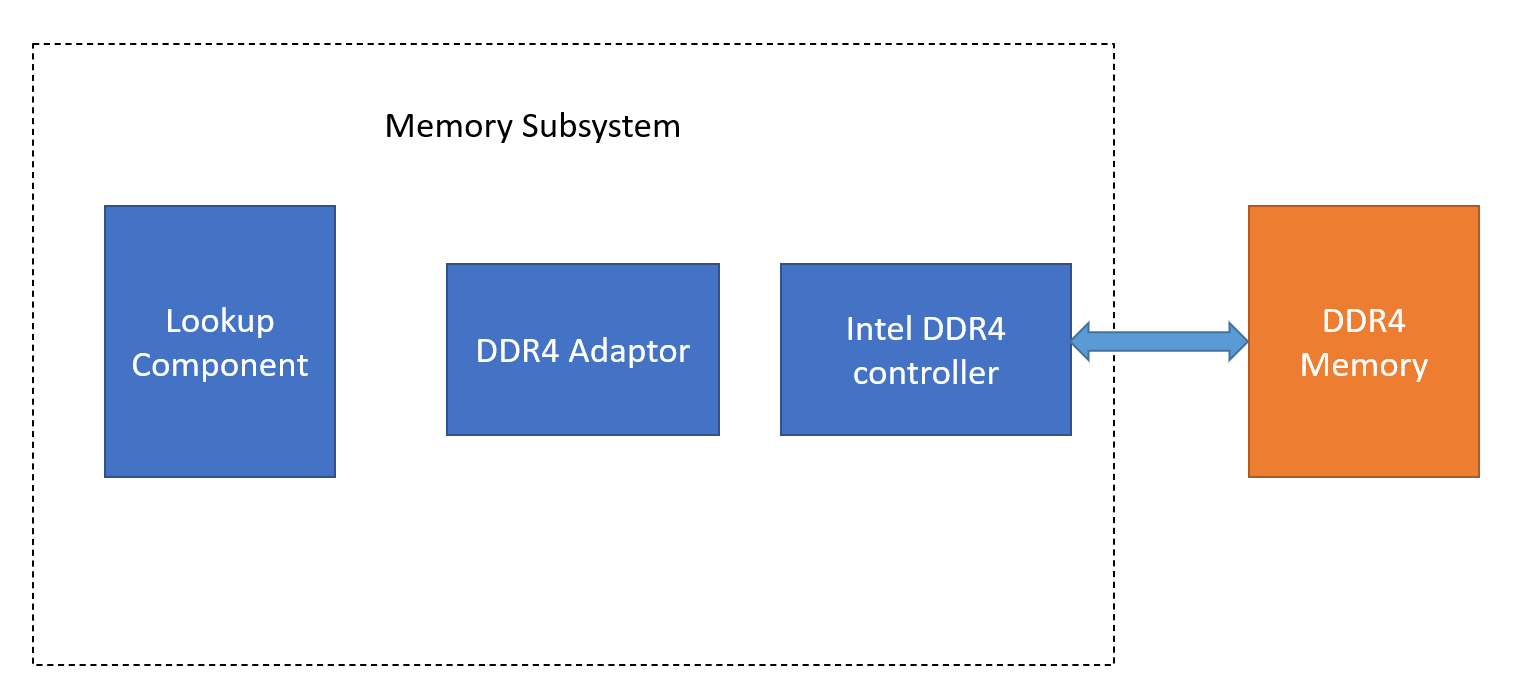
- Up to 8 lookup IP instances.
- Up to 8 EMIF instances.
- A memory controller that implements all the memory commands and protocol-level requirements.
- A soft logic adapter to boost memory throughput by traffic shaping.

You can configure the memory subsystem IP for use in various applications such as full crossbar for machine learning, multi-hierarchy memory bridge, or as a memory-specific adaptor with lookup core logic. All the available modes offer common scalability and compose-ability.
