Visible to Intel only — GUID: upx1665758713255
Ixiasoft
Visible to Intel only — GUID: upx1665758713255
Ixiasoft
3. Memory Subsystem IP Architecture and Feature Description
Memory subsystem build flow automatically identifies and connects subsystem internal building blocks to form the base subsystem and likewise for extended/vertical subsystem. For example, a memory base subsystem would automatically identify and connect the specific calibration block to the external memory instance(s) according to your specified subsystem placement of the physical external memory instance(s). The subsystem infrastructure comprises foundational IPs and standard protocol busses over an AXI interface.
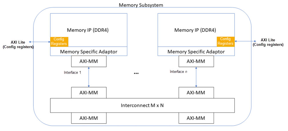
The following figure shows the subsystem IP block diagram, with important blocks and their connections:

Each memory subsystem can contain single or multiple instances of memory IPs. You can connect subsystems with multiple IPs through the Platform Designer Interconnect. The subsystems can contain 0 or more lookup IPs and single or multiple user interfaces (AXI-MM). Each interface has dedicated clock and reset domains.
Although each usage has unique requirements, the subsystems share scalability, composeability, and a certain degree of infrastructure.