Visible to Intel only — GUID: sam1412661908919
Ixiasoft
Visible to Intel only — GUID: sam1412661908919
Ixiasoft
VFIFO, LFIFO, and Read FIFO
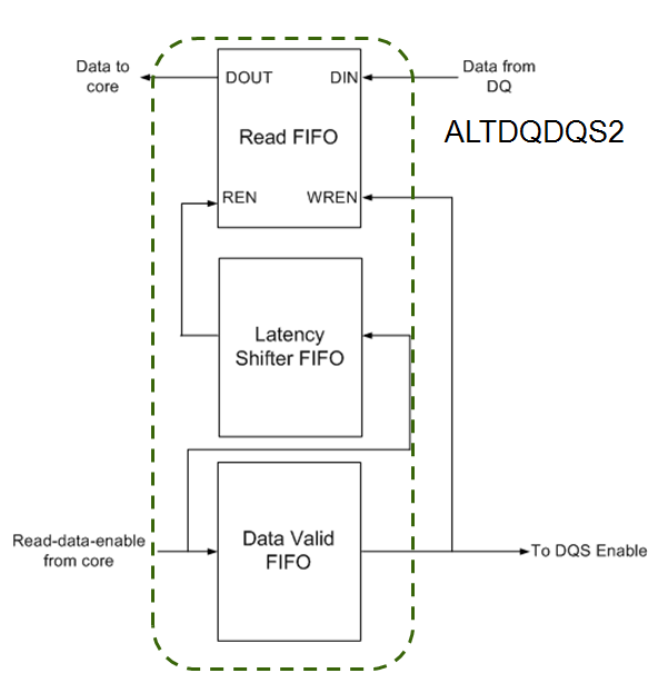
In Arria V and Cyclone V devices, the data valid FIFO (VFIFO) generates the input signal to the DQS_ENABLE_CTRL block and connects to the write enable port of the read FIFO. The latency shifter FIFO (LFIFO) connects to the read enable port of the read FIFO. The LFIFO and VFIFO implement each configurable latencies to determine the time to read enable and write enable for the Read FIFO respectively. The lfifo_rd_latency signal determines the latency setting in the LFIFO while the vfifo_inc_wr_ptr signal determines the latency setting for the VFIFO. The read FIFO is in every input data paths, and you can set the read FIFO to control the conversion between FR-FR or FR-HR in Arria V and Cyclone V devices.

When the host sends out a read command, a token is also sent to the LFIFO and the VFIFO. This token should be asserted for the length of the desired read burst. This token is referred to lfifo_rdata_en_full (for LFIFO) and vfifo_qvld (for VFIFO). In this testbench, the lfifo_rd_latency is set to 15d. Note that this is consistent with the latency noticed between rdataenfull of the LFIFO and readenable of the read FIFO, which is 16 half- rate clock cycles. The lfifo_rdata_en_full and vfifo_qvld signals pass through each HR-FR DDIO before it reaches the rdataenfull of the LFIFO and the qvldin of the VFIFO at 9.355 ms. The delayed qvldreg of the VFIFO (1.5 half-rate cycles) feeds the DQSENABLEIN of the DQS_ENABLE_CTRL block. Meanwhile, the rden signal of the LFIFO, which is delayed by 16 half-rate cycles, feeds the READENABLE of the read FIFO.
The dqsenable signal is asserted at 9.3825 ms. Edge-aligned input data starts at 9.385 ms and ends at 9.445 ms. The dqsenable signal is deasserted at 9.44 ms. In an actual application, you are required to have some form of DQS enable runtime calibration to obtain the correct DQS gating-ungating window. The strobe_io signal goes to Hi-Z when the DQS read operation completes. Because the writeenable signal of the read FIFO is always asserted, data is written into the read FIFO whenever the read FIFO is available, which is as early as 9.395 ms. However, data is only read out when the readenable signal is asserted between 9.515 ms and 9.575 ms. The data are available in the read_data_out signal. You can further optimize the timing to read the read FIFO by adjusting the LFIFO latency delay to create sufficient space between the read and write pointers in the read FIFO to maximize the throughput.
