Visible to Intel only — GUID: sam1412661792704
Ixiasoft
Visible to Intel only — GUID: sam1412661792704
Ixiasoft
Hard Read FIFO
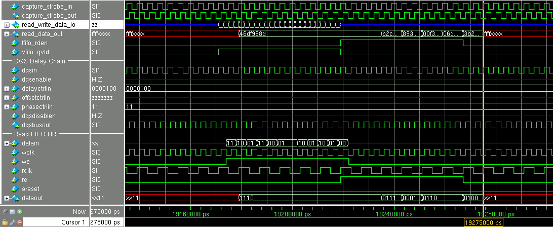
As seen in the waveform below, the incoming read data is available on read_write_data_io between 19.171 ms and 19.219 ms. The capture DDlO block captures input data (DQ) on the rising and falling edges of the capture clock (DQS). For Stratix V devices, the capture DDlO block feeds the hard read FlFO or bypasses the hard read FlFO and goes directly to the core. The data transfer from the capture DDlO block and the next stage is referred to as zero-cycle transfer. This means that the transfer must happen on the same clock edge.
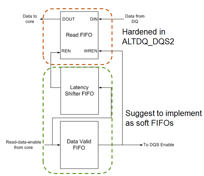
This design example uses a hard read FIFO. When the first data is available at 19.174 ms, the v/i/o_qvld is asserted. This signal passes through the write_enable_ctrl of the DDlO OUT before driving the read enable port of the read FIFO. As the write enable signal of the read FlFO block is asserted, data is written to the read FlFO between 19.174 ms and 19.222 ms . The l/i/o_rden, which is connected to the read enable port of the read FlFO block through a fifo_enable block, is then asserted between 19.219 ms and 19.267 ms. Read data is available in the core between 19.179 ms and 19.275 ms on read_data_out. You may further optimize the timing to read the read FlFO by adjusting the lfifo_rden to create enough space between the read and write pointers in the read FlFO to maximize the throughput.

