Visible to Intel only — GUID: fqw1481216717774
Ixiasoft
Visible to Intel only — GUID: fqw1481216717774
Ixiasoft
5.2.4.3.1. Hardware Design
The following sections describe a step-by-step method for building a bootable system for a Nios® II processor application copied from general purpose QSPI flash to RAM using a boot copier. The example below is designed based on Intel® MAX® 10 FPGA development kit.
IP Component Settings
- Create your Nios® II Processor Project using Intel® Quartus® Prime and Platform Designer.
- Ensure the Generic Serial Flash Interface IP is added into your Platform Designer system.
Figure 130. Connection for Generic Serial Flash Interface IPImportant:Figure 131. Generic Serial Flash Interface Parameter Settings
- Open Generic Serial Flash Interface parameter editor. Change the Device Density (Mb) according to the QSPI flash size.
- To access general purpose QSPI flash, enable Disable dedicated Active Serial Interface and Enable SPI pins interface.
- Change the addressing mode by modifying bit 8 of the Control Register value in the Default Settings parameter section. Changing bit 8 to 0x0 enables 3-byte addressing, or 0x1 enables 4-byte addressing.
Note: The 4-byte addressing mode is supported in the Intel® MAX® 10 FPGA Development Kit with Micron N25Q512A83GSF40F devices.
Prior to Intel® Quartus® Prime Pro Edition Version 19.3 and Intel® Quartus® Prime Standard Edition Version 20.1, the Control Register is available after you select Show Hidden Parameter by right clicking on the parameter editor.
- If you want to enable dual images configuration, ensure that Dual Configuration IP is instantiated in your Platform Designer system.
Note: Dual Images Configuration is only available in Intel® MAX® 10 devicesFigure 132. Dual Configuration IP
Reset and Exception Vector Settings for Nios II Using Boot Copier Method
- In the Nios® II Processor parameter editor, set the Reset Vector Memory to QSPI Flash and Exception Vector Memory to OCRAM/ External RAM.
Figure 133. Nios® II Parameter Editor Settings
- For dual configuration images in Intel® MAX® 10 devices, there are two Nios® II application data (HEX file) stored into the QSPI. Reset vector memory offset has to set correctly for the configuration images to call up the correct HEX data.
- Set Reset vector memory offset of the Nios® II Processor in first Platform Designer design to address 0x00000000.
- Set Reset vector memory offset of the Nios® II Processor in second Platform Designer design to another address to avoid overlapping. For example: Address 0x02000000 which is half of the QSPI memory size (512 Mb).
Figure 134. Reset Vector Offset Setting for First Platform Designer DesignFigure 135. Reset Vector Offset Setting for Second Platform Designer Design
- Click Generate HDL, the Generation dialog box appears.
- Specify output file generation options and then click Generate.
Intel Quartus Prime Software Settings
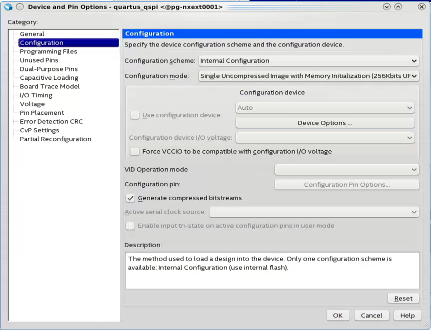
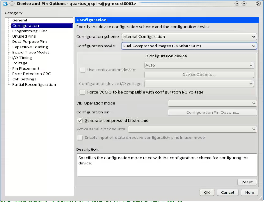
For Intel® MAX® 10 devices, there will be an option for Single Configuration Image and Dual Configuration Image:
- In the Intel® Quartus® Prime software, click on Assignment > Device > Device and Pin Options > Configuration. Set Configuration mode to Single Uncompressed Image or Single Compressed Image.
Note:
Intel® MAX® 10 only supports Single Uncompressed Image with Memory Initialization
Figure 136. Single Configuration Mode Selection in Intel® Quartus® Prime Software
- If you want to set it to Dual Configuration Image, in the Intel® Quartus® Prime software, click on Assignment -> Device -> Device and Pin Options -> Configuration. Set Configuration mode to Dual Compressed Images.
Figure 137. Dual Configuration Mode Selection in Intel® Quartus® Prime Software

- Click OK to exit the Device and Pin Options window.
- Click OK to exit the Device window.
- Click Start Compilation to compile your project.