Visible to Intel only — GUID: iga1464289981587
Ixiasoft
Visible to Intel only — GUID: iga1464289981587
Ixiasoft
7.5.5.4. Connect and Position the Tightly Coupled Memories
To associate the masters with the tightly coupled memories, perform the following steps:
- To facilitate creating connections between the tightly coupled memory and the Nios® II processor, click each new tightly coupled memory and click Move Up to move the individual memories just below the cpu component.
- If necessary, click the + to expand the tightly_coupled_instruction_memory component.
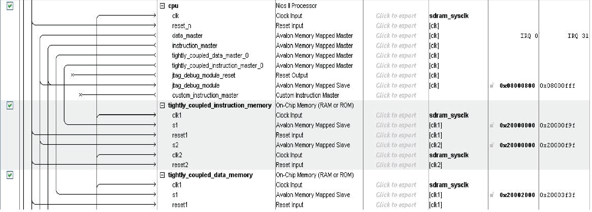
- Using the connections panel in Platform Designer, connect the s1 port of tightly_coupled_instruction_memory to the tightly_coupled_instruction_master_0 component listed under the cpu component. To connect a port, click the empty dot at the intersection of the s1 port and the port you want to connect.
- Similarly, connect the s2 port of tightly_coupled_instruction_memory to the cpu data_master port. This connection is shown in Figure 280 as the Avalon® -MM connection between the Avalon® -MM data master port and the Avalon® -MM slave port on the tightly coupled instruction memory. Port s2 of this dual-port memory is an Avalon® -MM slave port, not a tightly coupled slave port because s2 connects to an Avalon® -MM master, which is not a tightly coupled master.
- If necessary, click the + to expand the tightly_coupled_data_memory component.
- Connect the s1 port of tightly_coupled_data_memory to tightly_coupled_data_master_0.
- To change the tightly coupled memories to the same clock domain as the cpu, follow these steps:
- Click in the Clock column next to clk1 and clk2 for the s1 and s2 ports, respectively, of tightly_coupled_instruction_memory. A list of available clock signals appears.
- Select the same clock domain as the cpu from the list of available clocks to connect this clock to the slave ports.
- Similarly, connect reset1 and reset2 for the s1 and s2 ports, respectively, to clk_reset of the clock source.
- Repeat steps a-c for tightly_coupled_data_memory.
- In the Base column, enter the base addresses in the table below for all tightly coupled memories.
Table 59. Base Addresses for Tightly Coupled Memories Port Base tightly_coupled_instruction_memory s1 0x20000000 tightly_coupled_instruction_memory s2 0x20000000 tightly_coupled_data_memory s2 0x20002000 The end addresses automatically update to reflect the memory size that you specified in the configuration wizard. The base address specification is important. Tightly coupled memories must be mapped so that their addresses do not overlap with the embedded processor’s memories and peripherals that are connected to its Avalon® -MM instruction and data masters.
Figure 281. Connections for Tightly Coupled Memories
To simplify address decoding, map the high-order address bit to a unique location. By limiting the decoding logic to one bit, you minimize the effect of address decoding on fMAX. The Nios® II component works correctly even if the address map is not optimal; however, it displays a warning during system generation.
As an example of optimal address mapping, if all the normal memories and peripherals in your system occupy addresses below 0x2000000, mapping your tightly coupled memories at addresses from 0x2000000 and above satisfies this requirement.
- To set the exception address of the Nios® II processor, open the Nios® II processor’s configuration wizard. On the Core Nios® II tab, in the Exception vector memory: list, select tightly_coupled_instruction_memory_s1.
The address Offset fields are populated automatically and are indexed from the base address specified for the memory module on the System Contents tab.