Visible to Intel only — GUID: iga1447717590081
Ixiasoft
Visible to Intel only — GUID: iga1447717590081
Ixiasoft
3.4.4.2. ARM BE-32 Bus Byte Ordering
Some ARM cores use a bus byte ordering commonly referred to as big endian 32 (BE-32). BE-32 processor cores use a descending bit ordering when the masters are connected to the interconnect. For example, an ARM BE-32 processor core labels the data bits 31 down to 0. Such a processor core considers bits 31 down to 24 as byte offset 0. This layout differs from the Avalon® -MM specification, which defines byte 0 as data bits 7 down to 0.
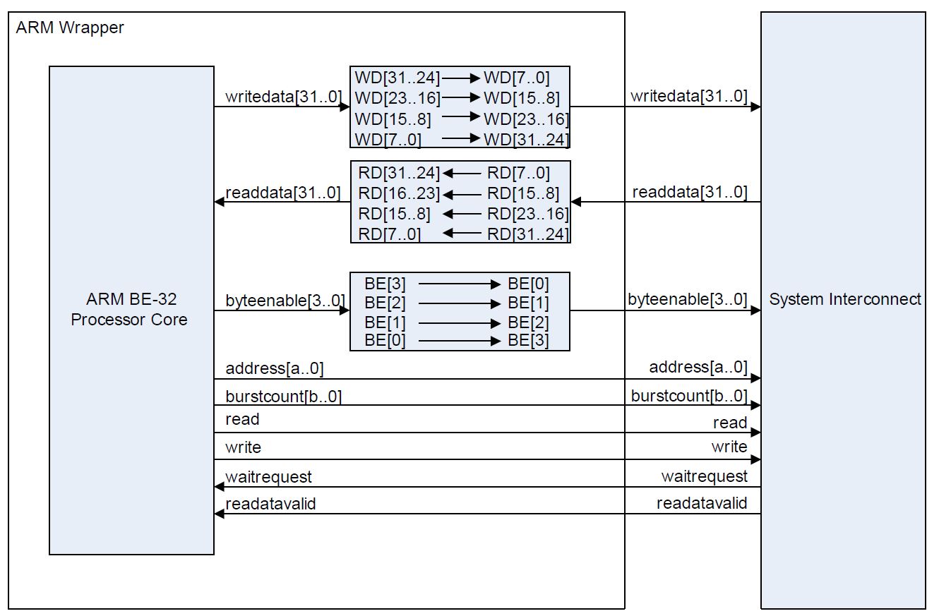
A BE-32 processor core accesses memory using the bus mapping shown below.
| Access Size (Bits) | Offset (Bytes) | Value | Byte Enable (Bits 3:0) | Write Data (Bits 31:24) | Write Data (Bits 23:16) | Write Data (Bits 15:8) | Write Data (Bits 7:0) |
|---|---|---|---|---|---|---|---|
| 8 | 0 | 0x0A | 1000 | 0x0A | — | — | — |
| 8 | 1 | 0x0A | 0100 | — | 0x0A | — | — |
| 8 | 2 | 0x0A | 0010 | — | — | 0x0A | — |
| 8 | 3 | 0x0A | 0001 | — | — | — | 0x0A |
| 16 | 0 | 0x0A0B | 1100 | 0x0A | 0x0B | — | — |
| 16 | 2 | 0x0A0B | 0011 | — | — | 0x0A | 0x0B |
| 32 | 0 | 0x0A0B0C0D | 1111 | 0x0A | 0x0B | 0x0C | 0x0D |
The write access behavior of the BE-32 processor shown in the table above differs greatly from the Nios® II processor behavior shown in Table 3. The only consistent access is the full 32-bit write access. In all the other cases, each processor accesses different byte lanes of the interconnect.
To connect a processor with BE-32 bus byte ordering to the interconnect, rename each byte lane as the figure below shows.
