External Memory Interfaces Intel Agilex® 7 M-Series FPGA IP User Guide
A newer version of this document is available. Customers should click here to go to the newest version.
Visible to Intel only — GUID: prf1693106337020
Ixiasoft
Visible to Intel only — GUID: prf1693106337020
Ixiasoft
7.3.7.2. Routing Guidelines for DDR5 Memory Down: 1 Rank or 2 Rank (x8 bit or x16 bit) Configurations
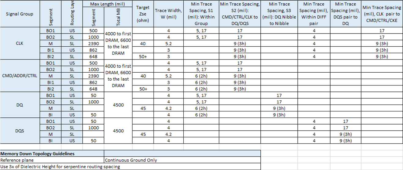
For example, the maximum length of the main trace routing can be derived from total trace length by subtracting the break-out and break-in trace segment lengths routed.
In this table, the signal trace width and minimum spacing/gaps (in mils) from edge-to-edge of signal traces are based on the default stackup shown in the PCB Stack-up and Design Considerations topic; however, PCB designers can use the target impedance for any other stackups. The h in the table indicates the minimum substrate height from signal layer to reference layer.

|
Reset signal routing also follows the CMD/ADD/CTRL routing design. Maintain an edge-to-edge space between the Reset signal and other signals on the same layer of at least 5x h. There is no requirement to have skew matching between the Reset signal and CLK signal.
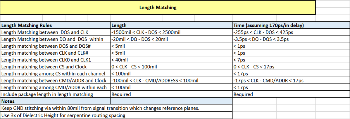
The following table provides a detailed skew matching guideline. Ensure that you include both PCB physical routing skew and package routing skew in your skew matching criteria. The physical length matching criteria in the table reflects the default stackup in our platform PCB design.

|
The maximum data rate depends on the memory configuration as shown in the following table.
Board thickness in the design can vary from thin to thick. In this design guideline, a standard thin board is 65 mil and 120 mil is a standard thick board.
| Memory Interface | DDR5 | |
|---|---|---|
| Signal Group | DQ | |
| Board Thickness (mil) | 65 mil or HDI or 120 mil (Data Routing must be on upper layers to avoid long via/vertical Xtalk) | 65 mil or HDI or 120 mil (Data Routing must be on upper layers to avoid long via/vertical Xtalk) |
| PCB Stripline Trace Impedance (ohms) | 45 | 45 |
| Memory Configuration | Memory Down | Memory Down |
| # of Rank | 1 (40bits total), x8 or x16 | 2 (40 bits total), x8 or x16 |
| Maximum PCB Length Total (inches) to the DRAM | 4.5 | 4.5 |
| Note | Maximum package length in FPGA design is shorter than 34mm | |