Visible to Intel only — GUID: xez1693102211275
Ixiasoft
1. About the External Memory Interfaces Agilex™ 7 M-Series FPGA IP
2. Agilex™ 7 M-Series FPGA EMIF IP – Introduction
3. Agilex™ 7 M-Series FPGA EMIF IP – Product Architecture
4. Agilex™ 7 M-Series FPGA EMIF IP – End-User Signals
5. Agilex™ 7 M-Series FPGA EMIF IP – Simulating Memory IP
6. Agilex™ 7 M-Series FPGA EMIF IP – DDR4 Support
7. Agilex™ 7 M-Series FPGA EMIF IP – DDR5 Support
8. Agilex™ 7 M-Series FPGA EMIF IP – LPDDR5 Support
9. Agilex™ 7 M-Series FPGA EMIF IP – Timing Closure
10. Agilex™ 7 M-Series FPGA EMIF IP – Controller Optimization
11. Agilex™ 7 M-Series FPGA EMIF IP – Debugging
12. Agilex™ 7 FPGA EMIF IP - Mailbox Support
13. Document Revision History for External Memory Interfaces Agilex™ 7 M-Series FPGA IP User Guide
3.1.1. Agilex™ 7 M-Series EMIF Architecture: I/O Subsystem
3.1.2. Agilex™ 7 M-Series EMIF Architecture: I/O SSM
3.1.3. Agilex™ 7 M-Series EMIF Architecture: I/O Bank
3.1.4. Agilex™ 7 M-Series EMIF Architecture: I/O Lane
3.1.5. Agilex™ 7 M-Series EMIF Architecture: Input DQS Clock Tree
3.1.6. Agilex™ 7 M-Series EMIF Architecture: PHY Clock Tree
3.1.7. Agilex™ 7 M-Series EMIF Architecture: PLL Reference Clock Networks
3.1.8. Agilex™ 7 M-Series EMIF Architecture: Clock Phase Alignment
3.1.9. User Clock in Different Core Access Modes
4.1. IP Interfaces for External Memory Interfaces (EMIF) IP - DDR4 Component
4.2. IP Interfaces for External Memory Interfaces (EMIF) IP - DDR4 DIMM
4.3. IP Interfaces for External Memory Interfaces (EMIF) IP - DDR5 Component
4.4. IP Interfaces for External Memory Interfaces (EMIF) IP - DDR5 DIMM
4.5. IP Interfaces for External Memory Interfaces (EMIF) IP - LPDDR5
4.1.1. s0_axi4_clock_in for External Memory Interfaces (EMIF) IP - DDR4 Component
4.1.2. s0_axi4_ctrl_ready for External Memory Interfaces (EMIF) IP - DDR4 Component
4.1.3. core_init_n for External Memory Interfaces (EMIF) IP - DDR4 Component
4.1.4. s0_axi4 for External Memory Interfaces (EMIF) IP - DDR4 Component
4.1.5. s0_axi4lite_clock for External Memory Interfaces (EMIF) IP - DDR4 Component
4.1.6. s0_axi4lite_reset_n for External Memory Interfaces (EMIF) IP - DDR4 Component
4.1.7. s0_axi4lite for External Memory Interfaces (EMIF) IP - DDR4 Component
4.1.8. mem_0 for External Memory Interfaces (EMIF) IP - DDR4 Component
4.1.9. mem_ck_0 for External Memory Interfaces (EMIF) IP - DDR4 Component
4.1.10. mem_reset_n for External Memory Interfaces (EMIF) IP - DDR4 Component
4.1.11. oct_0 for External Memory Interfaces (EMIF) IP - DDR4 Component
4.1.12. ref_clk for External Memory Interfaces (EMIF) IP - DDR4 Component
4.2.1. s0_axi4_clock_out for External Memory Interfaces (EMIF) IP - DDR4 DIMM
4.2.2. s0_axi4_ctrl_ready for External Memory Interfaces (EMIF) IP - DDR4 DIMM
4.2.3. core_init_n for External Memory Interfaces (EMIF) IP - DDR4 DIMM
4.2.4. s0_axi4 for External Memory Interfaces (EMIF) IP - DDR4 DIMM
4.2.5. s0_axi4lite_clock for External Memory Interfaces (EMIF) IP - DDR4 DIMM
4.2.6. s0_axi4lite_reset_n for External Memory Interfaces (EMIF) IP - DDR4 DIMM
4.2.7. s0_axi4lite for External Memory Interfaces (EMIF) IP - DDR4 DIMM
4.2.8. mem_0 for External Memory Interfaces (EMIF) IP - DDR4 DIMM
4.2.9. mem_ck_0 for External Memory Interfaces (EMIF) IP - DDR4 DIMM
4.2.10. mem_reset_n for External Memory Interfaces (EMIF) IP - DDR4 DIMM
4.2.11. oct_0 for External Memory Interfaces (EMIF) IP - DDR4 DIMM
4.2.12. ref_clk for External Memory Interfaces (EMIF) IP - DDR4 DIMM
4.3.1. s0_axi4_clock_in for External Memory Interfaces (EMIF) IP - DDR5 Component
4.3.2. s0_axi4_ctrl_ready for External Memory Interfaces (EMIF) IP - DDR5 Component
4.3.3. core_init_n for External Memory Interfaces (EMIF) IP - DDR5 Component
4.3.4. s0_axi4 for External Memory Interfaces (EMIF) IP - DDR5 Component
4.3.5. s0_axi4lite_clock for External Memory Interfaces (EMIF) IP - DDR5 Component
4.3.6. s0_axi4lite_reset_n for External Memory Interfaces (EMIF) IP - DDR5 Component
4.3.7. s0_axi4lite for External Memory Interfaces (EMIF) IP - DDR5 Component
4.3.8. mem_0 for External Memory Interfaces (EMIF) IP - DDR5 Component
4.3.9. mem_ck_0 for External Memory Interfaces (EMIF) IP - DDR5 Component
4.3.10. mem_reset_n_0 for External Memory Interfaces (EMIF) IP - DDR5 Component
4.3.11. oct_0 for External Memory Interfaces (EMIF) IP - DDR5 Component
4.3.12. ref_clk for External Memory Interfaces (EMIF) IP - DDR5 Component
4.4.1. s0_axi4_ctrl_ready for External Memory Interfaces (EMIF) IP - DDR5 DIMM
4.4.2. s1_axi4_ctrl_ready for External Memory Interfaces (EMIF) IP - DDR5 DIMM
4.4.3. s0_axi4_clock_in for External Memory Interfaces (EMIF) IP - DDR5 DIMM
4.4.4. core_init_n for External Memory Interfaces (EMIF) IP - DDR5 DIMM
4.4.5. s0_axi4 for External Memory Interfaces (EMIF) IP - DDR5 DIMM
4.4.6. s1_axi4 for External Memory Interfaces (EMIF) IP - DDR5 DIMM
4.4.7. s0_axi4lite_clock for External Memory Interfaces (EMIF) IP - DDR5 DIMM
4.4.8. s0_axi4lite_reset_n for External Memory Interfaces (EMIF) IP - DDR5 DIMM
4.4.9. s0_axi4lite for External Memory Interfaces (EMIF) IP - DDR5 DIMM
4.4.10. s1_axi4lite_clock for External Memory Interfaces (EMIF) IP - DDR5 DIMM
4.4.11. s1_axi4lite_reset_n for External Memory Interfaces (EMIF) IP - DDR5 DIMM
4.4.12. s1_axi4lite for External Memory Interfaces (EMIF) IP - DDR5 DIMM
4.4.13. mem_0 for External Memory Interfaces (EMIF) IP - DDR5 DIMM
4.4.14. mem_1 for External Memory Interfaces (EMIF) IP - DDR5 DIMM
4.4.15. mem_reset_n for External Memory Interfaces (EMIF) IP - DDR5 DIMM
4.4.16. mem_ck_0 for External Memory Interfaces (EMIF) IP - DDR5 DIMM
4.4.17. mem_ck_1 for External Memory Interfaces (EMIF) IP - DDR5 DIMM
4.4.18. mem_i3c for External Memory Interfaces (EMIF) IP - DDR5 DIMM
4.4.19. oct_0 for External Memory Interfaces (EMIF) IP - DDR5 DIMM
4.4.20. oct_1 for External Memory Interfaces (EMIF) IP - DDR5 DIMM
4.4.21. ref_clk for External Memory Interfaces (EMIF) IP - DDR5 DIMM
4.5.1. s0_axi4_clock_in for External Memory Interfaces (EMIF) IP - LPDDR5
4.5.2. core_init_n for External Memory Interfaces (EMIF) IP - LPDDR5
4.5.3. s0_axi4_ctrl_ready for External Memory Interfaces (EMIF) IP - LPDDR5
4.5.4. s0_axi4 for External Memory Interfaces (EMIF) IP - LPDDR5
4.5.5. s1_axi4 for External Memory Interfaces (EMIF) IP - LPDDR5
4.5.6. s0_axi4lite_clock for External Memory Interfaces (EMIF) IP - LPDDR5
4.5.7. s0_axi4lite_reset_n for External Memory Interfaces (EMIF) IP - LPDDR5
4.5.8. s0_axi4lite for External Memory Interfaces (EMIF) IP - LPDDR5
4.5.9. mem_0 for External Memory Interfaces (EMIF) IP - LPDDR5
4.5.10. mem_ck_0 for External Memory Interfaces (EMIF) IP - LPDDR5
4.5.11. mem_1 for External Memory Interfaces (EMIF) IP - LPDDR5
4.5.12. mem_ck_1 for External Memory Interfaces (EMIF) IP - LPDDR5
4.5.13. mem_reset_n for External Memory Interfaces (EMIF) IP - LPDDR5
4.5.14. oct_0 for External Memory Interfaces (EMIF) IP - LPDDR5
4.5.15. oct_1 for External Memory Interfaces (EMIF) IP - LPDDR5
4.5.16. ref_clk for External Memory Interfaces (EMIF) IP - LPDDR5
6.3.4.1. Address and Command Pin Placement for DDR4
6.3.4.2. DDR4 Data Width Mapping
6.3.4.3. General Guidelines - DDR4
6.3.4.4. x4 DIMM Implementation
6.3.4.5. Specific Pin Connection Requirements
6.3.4.6. Command and Address Signals
6.3.4.7. Clock Signals
6.3.4.8. Data, Data Strobes, DM/DBI, and Optional ECC Signals
6.4.5.1. Single Rank and Dual Rank x 8 Discrete (Component) Topology
6.4.5.2. Single Rank x16 and Dual Rank x16 Discrete (Component) Topology
6.4.5.3. ADDR/CMD Reference Voltage/RESET Signal Routing Guidelines for Single Rank x 8 and Single Rank x 16 Discrete (Component) Topologies
6.4.5.4. Skew Matching Guidelines for DDR4 Discrete Configurations
6.4.5.5. Power Delivery Recommendations for DDR4 Discrete Configurations
6.4.5.6. Agilex™ 7 M-Series EMIF Pin Swapping Guidelines
7.1. External Memory Interfaces (EMIF) IP - DDR5 Component Parameter Descriptions
7.2. External Memory Interfaces (EMIF) IP - DDR5 DIMM Parameter Descriptions
7.3. PHY DFE Tap Bias Values for DDR5
7.4. MEM DFE Tap Bias Values for DDR5
7.5. Agilex™ 7 M-Series FPGA EMIF IP Pin and Resource Planning
7.6. DDR5 Board Design Guidelines
7.6.1. PCB Stack-up and Design Considerations
7.6.2. General Design Considerations
7.6.3. DDR Differential Signals Routing
7.6.4. Ground Plane and Return Path
7.6.5. RDIMM, UDIMM, and SODIMM Break-in Layout Guidelines
7.6.6. DRAM Break-in Layout Guidelines
7.6.7. General Notes for EMIF Routing Guidelines Tables
7.6.8. DDR5 PCB Layout Guidelines
7.6.9. DDR5 RDIMM Power Management IC
7.6.10. DDR5 Simulation Strategy
7.6.8.1. DDR5 Discrete Component/Memory Down Topology: Single Rank x8 or x16, Dual Rank x8 or x16
7.6.8.2. Routing Guidelines for DDR5 Memory Down: Single Rank or Dual Rank (x8 bit or x16 bit) Configurations
7.6.8.3. Routing Guidelines for DDR5 RDIMM, UDIMM, and SODIMM Configurations
7.6.8.4. Example of a DDR5 layout on an Altera FPGA Platform Board
8.5.1. PCB Stack-up and Design Considerations
8.5.2. General Design Considerations
8.5.3. DDR Differential Signals Routing
8.5.4. Ground Plane and Return Path
8.5.5. DRAM Break-in Layout Guidelines
8.5.6. General Notes for EMIF Routing Guidelines Tables
8.5.7. LPDDR5 PCB Layout Guidelines
8.5.8. LPDDR5 Simulation Strategy
11.1. Interface Configuration Performance Issues
11.2. Functional Issue Evaluation
11.3. Timing Issue Characteristics
11.4. Verifying Memory IP Using the Signal Tap Logic Analyzer
11.5. Debugging with the External Memory Interface Debug Toolkit
11.6. Generating Traffic with the Test Engine IP
11.7. Guidelines for Developing HDL for Traffic Generator
11.8. Guidelines for Traffic Generator Status Check
Visible to Intel only — GUID: xez1693102211275
Ixiasoft
7.6.1. PCB Stack-up and Design Considerations
You can implement DDR5 interfaces with Type-III or Type-IV PCB stack-ups. A Type-III PCB with zero-built up layers and PTH vias which is used to implement a DDR4 design can also be used for DDR5 designs. Backdrill can be considered to reach higher supported DDR5 data rate. You can run simulation to determine whether backdrill is necessary.
A high-quality type-IV PCB with higher cost, uses not only plated-through-hole (PTH) vias to connect from the top to bottom layer, but also stacked vias, micro vias, and buried vias to connect between layers. The following figure shows a cross-sectional comparison of a PTH and stacked via.
Figure 32. Cross-sectional Comparison of Plated-Through Hole Via and Stacked Via
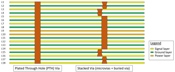
To support maximum data rate operation, DDR5 board design requires a high-quality PCB stackup using backdrill, micro vias, buried vias, or stacked vias to reduce crosstalk for high performance. Reducing the length of signal via is essential to minimizing the crosstalk between signals. You can perform simulation to determine whether to add backdrill or not based on your own stack-up.