Visible to Intel only — GUID: imp1693106245842
Ixiasoft
Visible to Intel only — GUID: imp1693106245842
Ixiasoft
7.3.7.1. DDR5 Discrete Component/Memory Down Topology: up to 40-Bit Interface (1 Rank x8 or x16, 2 Rank x8 or x16)
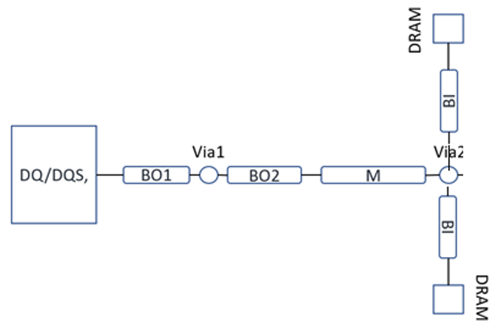
Data Group includes Data Strobe and its complement (DQS and DQS#), Data (DQ), and Data Mask (DM). The connection from the FPGA to DRAM is point-to-point topology as shown in the figure below, for single rank.

Double rank topology has clamshell/fly-by configuration, as shown in the figure below.

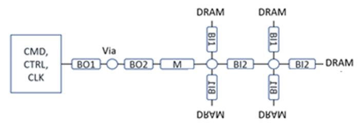
For address, command, control and clock signals, a fly-by or clamshell topology as shown in the figure below is recommended to meet signal-integrity performance and for easier routing. The termination approach for DDR5 is through programmable on-die-termination (ODT).


The above figures show examples of CA/CTL/CLK Fly-by clamshell routing topology for DDR5 memory down configuration.
Fly-by routing starts with the FPGA, then followed by DRAM chips daisy-chained together. The table in the following topic outlines routing guidelines for the command, control, and clock (CMD/CTRL, CLK) signals.