PCB Design Guidelines (HSSI, EMIF, MIPI, True Differential, PDN) User Guide: Agilex™ 5 FPGAs and SoCs
Visible to Intel only — GUID: oia1723798383560
Ixiasoft
Visible to Intel only — GUID: oia1723798383560
Ixiasoft
5.1. General DDR Signal Routing Guideline on PCB
General DDR Signal Routing Guideline on PCB
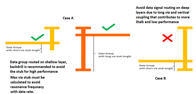
Altera recommends to route all data signals within a specific group on the same layer. Data Group signals (DQ, DM and DQS signals) are suggested to route on shallow layers (stripline or microstrip line) and use the shortest Z-height via transitions to avoid vertical crosstalk for better performance. Backdrilling can minimize the stub effect and achieve better performance, but this is not mandatory. You can run a simulation to determine whether to use backdrilling for deep layer routing. Long via stubs affects the channel ISI, however the impact of ISI is less than the impact of crosstalk for the max data rate performance.

To minimize horizontal crosstalk between signals on the same layer, it is recommended to maintain adequate signal trace-to-trace (edge to edge) space, with a minimum spacing of 3xH separation distance for inner layer, where H is the dielectric thickness to the closest reference plane as illustrated in the following figure. Refer to following routing guide sections for detailed spacing requirements for each signal group.

FPGA DDR FPGA Break Out Routing
Agilex™ 5 devices come with various pitch sizes for different FPGA pins. For VPBGA package devices breakout, it is recommended to use a dog bone configuration, stripline routing for inner GPIO pins fan-out and microstrip routing for GPIO pins at edge of the device, as suggested in General VPBGA PCB Layout Guideline section. For MBGA devices breakout, refer to MBGA PCB routing guidelines. Both stripline and microstrip routing guidelines are presented in this chapter for all supported EMIF interfaces and topologies.
DQS and CLK signals in the DDR interface are differential signals. It is recommended to route DQS/CLK as differential signals and use a symmetrical fan-out at the FPGA pin field.
The following figure shows the symmetrical routing of differential signals (DQS/CLK) at FPGA pin field and the length/skew matching between P/N lanes.
DRAM Break Out in Layout Routing
For discrete DRAM components on PCB, you can either use the dog-bone or via in pad at DRAM for the signal transition from inner layer to DRAM. If dog-bone via transition is used, it is recommended to separate them with larger pitch to avoid crosstalk between signal vias.
Symmetrical routing of differential signals (DQS/CLK) in the DRAM pin area is limited due to very small pitch. Altera recommends routing the differential signals as single-ended signals within the DRAM pin field, ensuring to keep the same impedance while changing from differential to single-ended configuration. Designers must also keep the same routing length for single-ended lane P and N single-ended lane within the DRAM pin field. Applying the skew matching between P/N lanes before reaching the DRAM pin field improves performance.
The following figure shows the single-ended routing for differential signals (DQS/CLK) at DRAM pin field when the pitch is very small along with skew matching.
Ground Plane and Return Path
A continuous and solid ground reference plane is crucial for data lines. Low impedance ground return path from the FPGA to DRAM devices should be provisioned. In addition, it is desirable to keep the distance between the ground stitching vias and signal transition within 80mils for better signal via return path and better signal integrity performance.
General Notes for EMIF Routing Guidelines Table
- All spacing requirements are the minimum requirement to be met on PCB in EMIF routing guidelines table.
- In the routing guideline table, h represents the trace-to-nearest-reference-plane height or distance. Board designer should use the formula in the routing guide table to calculate the correct spacing requirements.
- There is no differential impedance target for CLK and DQS. As a board designer, you should follow the EMIF routing table and keep traces closely coupled.
- The trace length and spacing in guideline table are based on FR-4 level PCB material and the PCB layout routing with the worst-case crosstalk. You can perform simulation if not following the requirements in the routing guide table.
- SL stands for stripline routing recommendation and US stands for upper surface (microstrip) routing recommendation in guideline tables.
- You need to design trace widths of BO, BO1, BO2 and BI based on the actual PCB stack-up and PCB design. It would be better if trace widths of BO, BO1, BO2 and BI can be designed closer to target impedance of the M segment.
- Include the FPGA package per-pin skew and PCB delay for skew matching.
- Does not require length matching on the Alert signal and Reset signal.
- Recommended to perform skew matching in time (picosecond).