Visible to Intel only — GUID: uxd1717612704548
Ixiasoft
1. About the External Memory Interfaces Agilex™ 7 M-Series FPGA IP
2. Agilex™ 7 M-Series FPGA EMIF IP – Introduction
3. Agilex™ 7 M-Series FPGA EMIF IP – Product Architecture
4. Agilex™ 7 M-Series FPGA EMIF IP – End-User Signals
5. Agilex™ 7 M-Series FPGA EMIF IP – Simulating Memory IP
6. Agilex™ 7 M-Series FPGA EMIF IP – DDR4 Support
7. Agilex™ 7 M-Series FPGA EMIF IP – DDR5 Support
8. Agilex™ 7 M-Series FPGA EMIF IP – LPDDR5 Support
9. Agilex™ 7 M-Series FPGA EMIF IP – Timing Closure
10. Agilex™ 7 M-Series FPGA EMIF IP – Controller Optimization
11. Agilex™ 7 M-Series FPGA EMIF IP – Debugging
12. Document Revision History for External Memory Interfaces Agilex™ 7 M-Series FPGA IP User Guide
3.1.1. Agilex™ 7 M-Series EMIF Architecture: I/O Subsystem
3.1.2. Agilex™ 7 M-Series EMIF Architecture: I/O SSM
3.1.3. Agilex™ 7 M-Series EMIF Architecture: I/O Bank
3.1.4. Agilex™ 7 M-Series EMIF Architecture: I/O Lane
3.1.5. Agilex™ 7 M-Series EMIF Architecture: Input DQS Clock Tree
3.1.6. Agilex™ 7 M-Series EMIF Architecture: PHY Clock Tree
3.1.7. Agilex™ 7 M-Series EMIF Architecture: PLL Reference Clock Networks
3.1.8. Agilex™ 7 M-Series EMIF Architecture: Clock Phase Alignment
3.1.9. User Clock in Different Core Access Modes
4.1.1. ref_clk for External Memory Interfaces (EMIF) IP
4.1.2. core_init_n for External Memory Interfaces (EMIF) IP
4.1.3. usr_async_clk for External Memory Interfaces (EMIF) IP
4.1.4. usr_clk for External Memory Interfaces (EMIF) IP
4.1.5. usr_rst_n for External Memory Interfaces (EMIF) IP
4.1.6. s0_axi4 for External Memory Interfaces (EMIF) IP
4.1.7. mem for External Memory Interfaces (EMIF) IP
4.1.8. oct for External Memory Interfaces (EMIF) IP
4.2.1. ref_clk for External Memory Interfaces (EMIF) IP
4.2.2. core_init_n for External Memory Interfaces (EMIF) IP
4.2.3. usr_async_clk for External Memory Interfaces (EMIF) IP
4.2.4. usr_clk for External Memory Interfaces (EMIF) IP
4.2.5. usr_rst_n for External Memory Interfaces (EMIF) IP
4.2.6. s0_axi4 for External Memory Interfaces (EMIF) IP
4.2.7. mem for External Memory Interfaces (EMIF) IP
4.2.8. i3c for External Memory Interfaces (EMIF) IP
4.2.9. mem_lbd for External Memory Interfaces (EMIF) IP
4.2.10. mem_lbs for External Memory Interfaces (EMIF) IP
4.2.11. oct for External Memory Interfaces (EMIF) IP
4.3.1. ref_clk for External Memory Interfaces (EMIF) IP
4.3.2. core_init_n for External Memory Interfaces (EMIF) IP
4.3.3. usr_async_clk for External Memory Interfaces (EMIF) IP
4.3.4. usr_clk for External Memory Interfaces (EMIF) IP
4.3.5. usr_rst_n for External Memory Interfaces (EMIF) IP
4.3.6. s0_axi4 for External Memory Interfaces (EMIF) IP
4.3.7. mem for External Memory Interfaces (EMIF) IP
4.3.8. oct for External Memory Interfaces (EMIF) IP
6.2.4.1. Address and Command Pin Placement for DDR4
6.2.4.2. DDR4 Data Width Mapping
6.2.4.3. General Guidelines - DDR4
6.2.4.4. x4 DIMM Implementation
6.2.4.5. Specific Pin Connection Requirements
6.2.4.6. Command and Address Signals
6.2.4.7. Clock Signals
6.2.4.8. Data, Data Strobes, DM/DBI, and Optional ECC Signals
6.3.5.1. Single Rank x 8 Discrete (Component) Topology
6.3.5.2. Single Rank x 16 Discrete (Component) Topology
6.3.5.3. ADDR/CMD Reference Voltage/RESET Signal Routing Guidelines for Single Rank x 8 and Single Rank x 16 Discrete (Component) Topologies
6.3.5.4. Skew Matching Guidelines for DDR4 Discrete Configurations
6.3.5.5. Power Delivery Recommendations for DDR4 Discrete Configurations
6.3.5.6. Agilex™ 7 M-Series EMIF Pin Swapping Guidelines
7.3.1. PCB Stack-up and Design Considerations
7.3.2. General Design Considerations
7.3.3. DDR Differential Signals Routing
7.3.4. Ground Plane and Return Path
7.3.5. RDIMM, UDIMM, and SODIMM Break-in Layout Guidelines
7.3.6. DRAM Break-in Layout Guidelines
7.3.7. DDR5 PCB Layout Guidelines
7.3.8. DDR5 Simulation Strategy
7.3.7.1. DDR5 Discrete Component/Memory Down Topology: up to 40-Bit Interface (1 Rank x8 or x16, 2 Rank x8 or x16)
7.3.7.2. Routing Guidelines for DDR5 Memory Down: 1 Rank or 2 Rank (x8 bit or x16 bit) Configurations
7.3.7.3. Routing Guidelines for DDR5 RDIMM, UDIMM, and SODIMM Configurations
7.3.7.4. Example of a DDR5 layout on an Altera FPGA Platform Board
11.1. Interface Configuration Performance Issues
11.2. Functional Issue Evaluation
11.3. Timing Issue Characteristics
11.4. Verifying Memory IP Using the Signal Tap Logic Analyzer
11.5. Debugging with the External Memory Interface Debug Toolkit
11.6. Generating Traffic with the Test Engine IP
11.7. Guidelines for Developing HDL for Traffic Generator
11.8. Guidelines for Traffic Generator Status Check
Visible to Intel only — GUID: uxd1717612704548
Ixiasoft
11.8.1. Status Check Using the Signal Tap Logic Analyzer
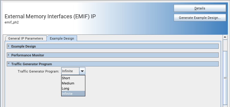
When you generate an Agilex™ 7 FPGA EMIF IP design example, you can specify the traffic pattern to run. Select the required setting, as illustrated in the figure below.
Figure 83. Selecting Traffic Generator Pattern


Refer to the External Memory Interfaces Agilex™ 7 M-Series FPGA IP Design Example User Guide for more information.
Observing Status with the Signal Tap Logic Analyzer
Follow these steps to observe status using the Signal Tap Logic Analyzer:
- Generate a Signal Tap Logic Analyzer file, which includes traffic generator status signals.
Figure 84.
 Note: The status_done and status_error ports on the traffic_generator|hydra_inst|global_csr instance are the traffic generator status signals.
 - Save and enable the Signal Tap file in the project, and recompile the design.
- Configure the device with your .sof file and observe the signals status through signal tap file.
- Signal values of status_done=1 and status_error=0 indicate that the traffic test completed with no traffic errors.
Figure 85.
 Note: For an infinite traffic pattern program, you will not see status_done=1, because the traffic continues running. Set the trigger conditions at the rising edge of the status_error signal and let the traffic run. Any failure in traffic is detected if the status_error signal goes high.