External Memory Interfaces Agilex™ 7 M-Series FPGA IP User Guide
A newer version of this document is available. Customers should click here to go to the newest version.
Visible to Intel only — GUID: luy1693244616234
Ixiasoft
Visible to Intel only — GUID: luy1693244616234
Ixiasoft
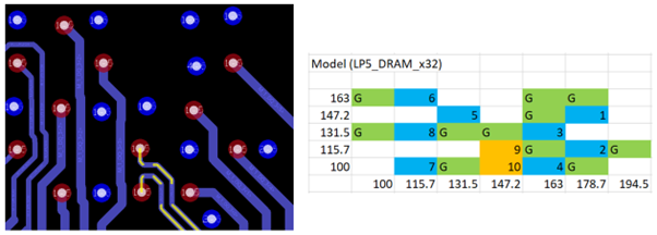
8.3.6.3. Example of an LPDDR5 Layout on an Altera® FPGA Platform Board
This example has been designed on a thick PCB (120mil stackup) using micro vias and through vias with backdrill. The LPDDR5 signal routing is on upper layers to avoid vertical crosstalk on interface and achieve high performance.
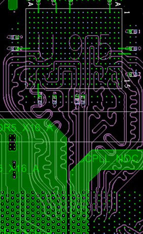
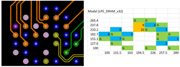
In addition, the following figure shows a LPDDR5 64-bit device board routing sample with pitch dimension of 0.4×0.4mm. The microvia has been used for via transitions on this interface.