External Memory Interfaces Agilex™ 7 M-Series FPGA IP User Guide
A newer version of this document is available. Customers should click here to go to the newest version.
Visible to Intel only — GUID: skp1693244524683
Ixiasoft
Visible to Intel only — GUID: skp1693244524683
Ixiasoft
8.3.6.1. LPDDR5 Discrete Component/Memory Down Topology (1 Rank or 2 Rank, up to 64 Bit Interface)
There are four DRAM interface signal groupings: Data Group, Command-Address Group, Control Group, and Clock Group. The connection between the FPGA and DRAM uses point-to-point topology for Data, Command/Address, Control, and Clocks, as shown in the following figure.

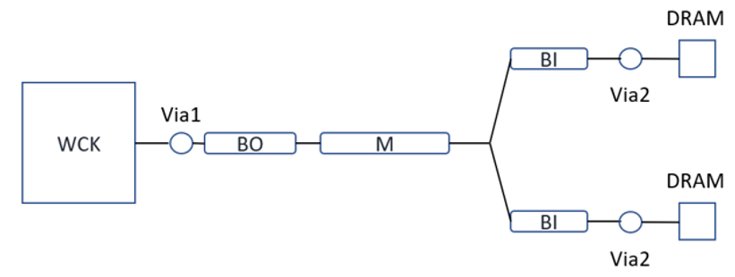
The LPDDR5 interface does not support a traditional dual-directional data-strobe architecture. However, two single-directional data strobes such as Write Clock (WCK) for Write Operations and an optional Read Clock (RDQS) for Read Operations are supported.
The following two figures show the connection topology for DQ, WCK signal and CA, CLK, CTRL signals for LPDDR5.

