Visible to Intel only — GUID: ece1693106431408
Ixiasoft
1. About the External Memory Interfaces Agilex™ 7 M-Series FPGA IP
2. Agilex™ 7 M-Series FPGA EMIF IP – Introduction
3. Agilex™ 7 M-Series FPGA EMIF IP – Product Architecture
4. Agilex™ 7 M-Series FPGA EMIF IP – End-User Signals
5. Agilex™ 7 M-Series FPGA EMIF IP – Simulating Memory IP
6. Agilex™ 7 M-Series FPGA EMIF IP – DDR4 Support
7. Agilex™ 7 M-Series FPGA EMIF IP – DDR5 Support
8. Agilex™ 7 M-Series FPGA EMIF IP – LPDDR5 Support
9. Agilex™ 7 M-Series FPGA EMIF IP – Timing Closure
10. Agilex™ 7 M-Series FPGA EMIF IP – Controller Optimization
11. Agilex™ 7 M-Series FPGA EMIF IP – Debugging
12. Document Revision History for External Memory Interfaces Agilex™ 7 M-Series FPGA IP User Guide
3.1.1. Agilex™ 7 M-Series EMIF Architecture: I/O Subsystem
3.1.2. Agilex™ 7 M-Series EMIF Architecture: I/O SSM
3.1.3. Agilex™ 7 M-Series EMIF Architecture: I/O Bank
3.1.4. Agilex™ 7 M-Series EMIF Architecture: I/O Lane
3.1.5. Agilex™ 7 M-Series EMIF Architecture: Input DQS Clock Tree
3.1.6. Agilex™ 7 M-Series EMIF Architecture: PHY Clock Tree
3.1.7. Agilex™ 7 M-Series EMIF Architecture: PLL Reference Clock Networks
3.1.8. Agilex™ 7 M-Series EMIF Architecture: Clock Phase Alignment
3.1.9. User Clock in Different Core Access Modes
4.1.1. ref_clk for External Memory Interfaces (EMIF) IP
4.1.2. core_init_n for External Memory Interfaces (EMIF) IP
4.1.3. usr_async_clk for External Memory Interfaces (EMIF) IP
4.1.4. usr_clk for External Memory Interfaces (EMIF) IP
4.1.5. usr_rst_n for External Memory Interfaces (EMIF) IP
4.1.6. s0_axi4 for External Memory Interfaces (EMIF) IP
4.1.7. mem for External Memory Interfaces (EMIF) IP
4.1.8. oct for External Memory Interfaces (EMIF) IP
4.2.1. ref_clk for External Memory Interfaces (EMIF) IP
4.2.2. core_init_n for External Memory Interfaces (EMIF) IP
4.2.3. usr_async_clk for External Memory Interfaces (EMIF) IP
4.2.4. usr_clk for External Memory Interfaces (EMIF) IP
4.2.5. usr_rst_n for External Memory Interfaces (EMIF) IP
4.2.6. s0_axi4 for External Memory Interfaces (EMIF) IP
4.2.7. mem for External Memory Interfaces (EMIF) IP
4.2.8. i3c for External Memory Interfaces (EMIF) IP
4.2.9. mem_lbd for External Memory Interfaces (EMIF) IP
4.2.10. mem_lbs for External Memory Interfaces (EMIF) IP
4.2.11. oct for External Memory Interfaces (EMIF) IP
4.3.1. ref_clk for External Memory Interfaces (EMIF) IP
4.3.2. core_init_n for External Memory Interfaces (EMIF) IP
4.3.3. usr_async_clk for External Memory Interfaces (EMIF) IP
4.3.4. usr_clk for External Memory Interfaces (EMIF) IP
4.3.5. usr_rst_n for External Memory Interfaces (EMIF) IP
4.3.6. s0_axi4 for External Memory Interfaces (EMIF) IP
4.3.7. mem for External Memory Interfaces (EMIF) IP
4.3.8. oct for External Memory Interfaces (EMIF) IP
6.2.4.1. Address and Command Pin Placement for DDR4
6.2.4.2. DDR4 Data Width Mapping
6.2.4.3. General Guidelines - DDR4
6.2.4.4. x4 DIMM Implementation
6.2.4.5. Specific Pin Connection Requirements
6.2.4.6. Command and Address Signals
6.2.4.7. Clock Signals
6.2.4.8. Data, Data Strobes, DM/DBI, and Optional ECC Signals
6.3.5.1. Single Rank x 8 Discrete (Component) Topology
6.3.5.2. Single Rank x 16 Discrete (Component) Topology
6.3.5.3. ADDR/CMD Reference Voltage/RESET Signal Routing Guidelines for Single Rank x 8 and Single Rank x 16 Discrete (Component) Topologies
6.3.5.4. Skew Matching Guidelines for DDR4 Discrete Configurations
6.3.5.5. Power Delivery Recommendations for DDR4 Discrete Configurations
6.3.5.6. Agilex™ 7 M-Series EMIF Pin Swapping Guidelines
7.3.1. PCB Stack-up and Design Considerations
7.3.2. General Design Considerations
7.3.3. DDR Differential Signals Routing
7.3.4. Ground Plane and Return Path
7.3.5. RDIMM, UDIMM, and SODIMM Break-in Layout Guidelines
7.3.6. DRAM Break-in Layout Guidelines
7.3.7. DDR5 PCB Layout Guidelines
7.3.8. DDR5 Simulation Strategy
7.3.7.1. DDR5 Discrete Component/Memory Down Topology: up to 40-Bit Interface (1 Rank x8 or x16, 2 Rank x8 or x16)
7.3.7.2. Routing Guidelines for DDR5 Memory Down: 1 Rank or 2 Rank (x8 bit or x16 bit) Configurations
7.3.7.3. Routing Guidelines for DDR5 RDIMM, UDIMM, and SODIMM Configurations
7.3.7.4. Example of a DDR5 layout on an Altera FPGA Platform Board
11.1. Interface Configuration Performance Issues
11.2. Functional Issue Evaluation
11.3. Timing Issue Characteristics
11.4. Verifying Memory IP Using the Signal Tap Logic Analyzer
11.5. Debugging with the External Memory Interface Debug Toolkit
11.6. Generating Traffic with the Test Engine IP
11.7. Guidelines for Developing HDL for Traffic Generator
11.8. Guidelines for Traffic Generator Status Check
Visible to Intel only — GUID: ece1693106431408
Ixiasoft
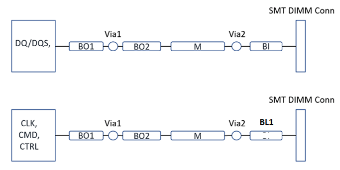
7.3.7.3. Routing Guidelines for DDR5 RDIMM, UDIMM, and SODIMM Configurations
The following figure shows DDR5 1 x DIMM per channel topology. A maximum of two transition vias are allowed for high performance.
Figure 48. DDR5 RDIMM, UDIMM, and SODIMM, 1 DIMM Per Channel Topology (1 Rank or 2 rank, x8 or x16 Bits, up to 40 Bits interface)
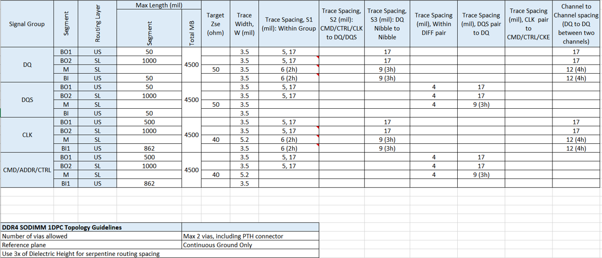
The following table shows physical trace segment routing guidelines, including the target impedance of routing for each signal and the minimum space between signal traces on the same layer. The column trace widths (in mil) and minimum space between traces (in mil) are based on a Altera board design stackup; however, the PCB designer must meet the impedance target criteria. The h in the routing guideline stands for the minimum substrate height between the signal layer and reference plane. Ensure that you follow the trace-to-trace-edge gap/space criteria in the guideline, based on “h” in various stackups.
|
Reset signal routing design also follows the command, address, and control (CMD/ADD/CTRL) routing design. Maintain the space from the Reset signal to other signals on the same layer (edge to edge) at least 5x h. There is no requirement to have skew matching between Reset and CLK signals.
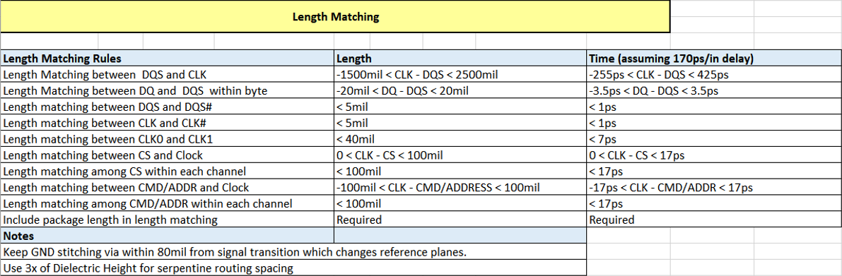
Skew matching for a DDR interface consists of both package routing skew and PCB physical routing skew. You must maintain skew matching of CA and CTRL with respect to the clock signals to ensure that signals at the receiver are correctly sampled. There is also a skew matching requirement for DQ and DQS within a byte group, DQS and CLK.
The following table provides a detailed skew matching guideline to facilitate PCB trace routing. The length matching criteria in this table represents a default PCB on an Altera platform board design. Skew matching criteria must be always followed in any other stackup.
|
The maximum DDR5 data rate depends on the configuration and PCB in the following table. For information on the maximum supported data rate, refer to the appropriate Agilex™ 7 FPGA device data sheet.
Board thickness in the design can vary from thin to thick. The 65 mil is a standard thin and 120 mil is a standard thick PCB in this design guideline.
| Memory Interface | DDR5 UDIMM | DDR5 RDIMM | DDR5 SODIMM |
|---|---|---|---|
| Signal group | DQ | ||
| Board Thickness (Thin or Thick) |
65 mil or HDI or 120mil (Data Routing must be on upper layers to avoid long via/vertical Xtalk) | 65 mil or HDI or 120mil (Data Routing must be on upper layers to avoid long via/vertical Xtalk) | 65mil or HDI or 120mil (Data Routing must be on upper layers to avoid long via/vertical Xtalk) |
| PCB Stripline Trace Impedance (ohms) | 50 | 50 | 50 |
| Memory Configuration | 1 xDIMM per Channel (40 Bits total), x8 or x16 | 1x DIMM per Channel (40 Bits total), x8 or x16 | 1x DIMM per Channel (40 bits total), x8 or x16 |
| # of Rank | 2 per DIMM | 2 per DIMM | 2 per DIMM |
| Max. Length Total (Inch) | 4.5 | 4.5 | 4.5 |
| Notes | Max. package length in FPGA design is shorter than 34mm. | ||