Visible to Intel only — GUID: wbu1506098666373
Ixiasoft
1.2.2.1.1. Device Selection Section
1.2.2.1.2. Power Rail Data and Configuration Section
1.2.2.1.3. Meeting Target Impedance when Entering 0 A into the PDN Tool
1.2.2.1.4. Dealing with Multiple Shared Power Supply Pin Types
1.2.2.1.5. VRM Data Section
1.2.2.1.6. Rail Group Summary Section
1.2.2.1.7. VRM Impedance Section
1.2.2.1.8. BGA Via Section
1.2.2.1.9. Plane Section
1.2.2.1.10. Spreading Section
1.2.2.1.11. Implementing Split Planes
1.2.2.1.12. FEFFECTIVE Section
1.2.2.1.13. Decoupling Section
1.2.2.1.14. Results Summary Section
1.2.2.1.15. Recommended Flow for Deriving Decoupling for an FPGA System using the System_Decap Tab
Visible to Intel only — GUID: wbu1506098666373
Ixiasoft
1.3.1.2. Inputting Stackup Data
- Click the Stackup tab.
- Input your stackup values for the following parameters:
- Number of Layers
- Drill Size
- BGA Via pitch
- Foil Thickness
- Select a dielectric material from the Dielectric Material drop-down menu.
Note: If you are using a custom dielectric material, skip this step and proceed to the Using a Custom Dielectric Material section.
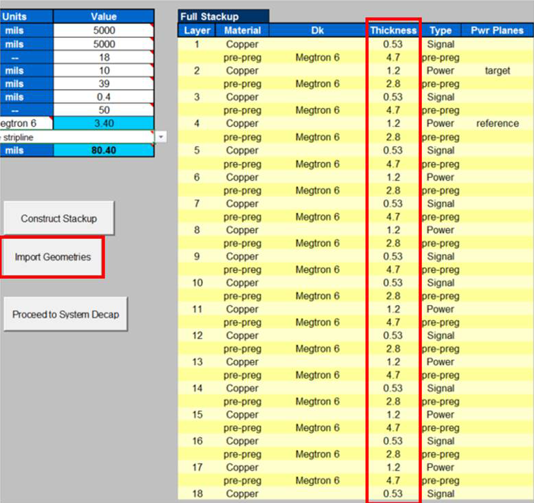
- Click Construct Stackup, then click Yes in the Construct Stackup confirmation dialog box.
The Full Stackup section updates based on your inputs.
- Enter the Thickness values for each layer in the Full Stackup table, then click Import Geometries.
Figure 23. Full Stackup Table

- Save your data to prevent data loss.
Related Information