Device-Specific Power Delivery Network (PDN) Tool 2.0 User Guide
ID
683293
Date
8/24/2021
Public
Visible to Intel only — GUID: zdh1506361144296
Ixiasoft
1.2.2.1.1. Device Selection Section
1.2.2.1.2. Power Rail Data and Configuration Section
1.2.2.1.3. Meeting Target Impedance when Entering 0 A into the PDN Tool
1.2.2.1.4. Dealing with Multiple Shared Power Supply Pin Types
1.2.2.1.5. VRM Data Section
1.2.2.1.6. Rail Group Summary Section
1.2.2.1.7. VRM Impedance Section
1.2.2.1.8. BGA Via Section
1.2.2.1.9. Plane Section
1.2.2.1.10. Spreading Section
1.2.2.1.11. Implementing Split Planes
1.2.2.1.12. FEFFECTIVE Section
1.2.2.1.13. Decoupling Section
1.2.2.1.14. Results Summary Section
1.2.2.1.15. Recommended Flow for Deriving Decoupling for an FPGA System using the System_Decap Tab
Visible to Intel only — GUID: zdh1506361144296
Ixiasoft
1.3.2.5. Calculating Plane
Based on your layer location assumption, the tool automatically calculates the plane R and C.
- Click the Stackup tab.
- Enter your expected plane length and width values in the Plane Length and Plane Width fields, respectively.
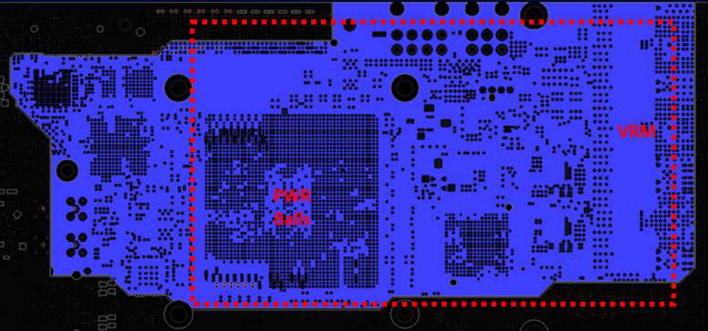
This is the best method for estimating if the layout design is already in progress (see the following figure).
Figure 29. Plane Size EstimationThe tool only measures the plane size from the VRM to the FPGA.
- Select which layers you want to use as target (power) and reference (ground, two layers maximum) in the Full Stackup table.
- Click Import Geometries on the left side of the Full Stackup table.
- Click the Plane_Cap tab.
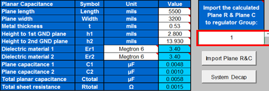
The tool automatically updates the plane parasitics.
- Change the regulator group number in the Import the calculated Plane R & Plane C to regulator Group field, then click Import Plane R&C.
Figure 30. Plane_Cap Table

- Click the System_Decap tab and verify that the tool has updated the parasitic.
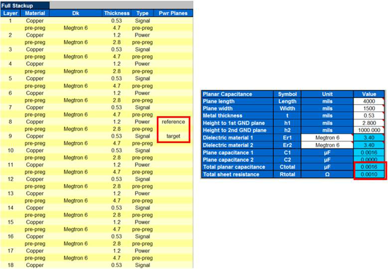
Note: The PDN tool does not support the multi-layered design for a single power. However, you can repeat 1 through 6 for each power layer, keeping the estimated parasitic numbers of each and combining capacitances of each power for final capacitance and calculating resistances of each power in parallel to get the final resistance. For example, if both layers nine and 10 of roughly the same size plane have one power rail, the tool calculates the parasitics based on one power and one reference layer in the Full Stackup table as shown in the figure below. Then, the final capacitance can be 0.0016 x 2 = 0.0032 µF and the final resistance can be 0.001 / 2 = 0.0005 Ω.Figure 31. Plane Parasitics
