Visible to Intel only — GUID: xkt1668432624841
Ixiasoft
1. About the Agilex™ 7 F-Series and I-Series FPGA Memory Subsystem IP
2. Introduction to Memory Subsystem IP
3. Memory Subsystem IP Architecture and Feature Description
4. Memory Subsystem Features
5. Memory Subsystem Interfaces and Signals
6. Memory Subsystem User Operations
7. Memory Subsystem Register Descriptions
8. Parameterizing the Memory Subsystem IP
9. Simulating a Design Example
10. Document Revision History for Agilex™ 7 F-Series and I-Series FPGA Memory Subsystem IP User Guide
5.3.1. TCAM AXI-ST Request Interface
5.3.2. TCAM AXI-ST Response Interface
5.3.3. TCAM AXI-Lite Interface
5.3.4. BCAM AXI-ST Request Interface
5.3.5. BCAM AXI-ST Response Interface
5.3.6. BCAM AXI-Lite Interface
5.3.7. MBL AXI-ST Request Interface
5.3.8. MBL AXI-ST Response Interface
5.3.9. MBL AXI-Lite Interface
6.4.1. MBL Flush Operation
6.4.2. MBL Insert Key Operation
6.4.3. MBL Delete Key Operation
6.4.4. MBL Lookup Operation Using Key
6.4.5. MBL Modify Operation
6.4.6. MBL Modify Result Using Handle Operation
6.4.7. MBL Delete Key Using Handle Operation
6.4.8. MBL Lookup Using Handle Operation
6.4.9. MBL Insert Key if Not Present or Modify Result if Present Operation
6.4.10. MBL Get Handle Operation
7.2.1. Offset 0x0000 Version
7.2.2. Offset 0x0004 Feature List
7.2.3. Offset 0x0010 Memory Interfaces 0-7
7.2.4. Offset 0x0014 Memory Interfaces 8-15
7.2.5. Offset 0x0018 Memory Interfaces 16-23
7.2.6. Offset 0x001C Memory Interfaces 24-31
7.2.7. Offset 0x0020 Scratch Pad
7.2.8. Offset 0x0030 Control Policy (Lower DWORD)
7.2.9. Offset 0x0034 Control Policy (Upper DWORD)
7.2.10. Offset 0x0038 Read Access Control Policy (Lower DWORD)
7.2.11. Offset 0x003C Read Access Control Policy (Upper DWORD)
7.2.12. Offset 0x0040 Write Access Control Policy (Lower DWORD)
7.2.13. Offset 0x0044 Write Access Control Policy (Upper DWORD)
7.2.14. Offset 0x0050 Memory Status Bitmask 0
7.2.15. Offset 0x0054 Memory Status Bitmask 1
7.2.16. Offset 0x0058 Memory Ready Status 0
7.2.17. Offset 0x005C Memory Ready Status 1
7.2.18. Offset 0x0060 Memory Error Status 0
7.2.19. Offset 0x0064 Memory Error Status 1
7.3.2.1. Version
7.3.2.2. Feature List
7.3.2.3. Interface Attribute Parameters
7.3.2.4. Interface Attribute Parameters 1
7.3.2.5. Scratch Pad
7.3.2.6. General Control (GEN_CTRL)
7.3.2.7. Management Control (MGMT_CTRL)
7.3.2.8. Hash function_0 seed
7.3.2.9. Hash function_1 seed
7.3.2.10. Hash function_2 seed
7.3.2.11. Warning 0 (WARNING_0)
7.3.2.12. Fatal Error (FATAL_ERROR_0)
7.3.2.13. Monitor 0 (MON_)
7.3.2.14. Total Entries (TOTAL_ENTRIES)
7.3.2.15. Max. Rehouse Iterations (Max_Rehouse_Iterations)
7.3.2.16. Statistics Control (STATS_CTRL)
7.3.2.17. Active Table Entries (TABLE_ENTRIES)
7.3.2.18. Key_N
7.3.2.19. Result_N
7.5.1. MBL DFH
7.5.2. General MBL Registers
7.5.3. Version
7.5.4. Mbl_scratch
7.5.5. Mbl_gen_ctrl
7.5.6. Mbl_mgmt_ctrl
7.5.7. Mbl_key_handle
7.5.8. Mbl_nxt_handle_req
7.5.9. Mbl_nxt_handle
7.5.10. Mbl_warning_0
7.5.11. Mbl_fatal_0
7.5.12. Mbl_mon_0
7.5.13. Mbl_total_entries
7.5.14. Mbl_total_rehashes
7.5.15. Mbl_max_used_bins
7.5.16. Mbl_stats_ctrl
7.5.17. Mbl_stats_result
7.5.18. Mbl_max_lkup_latency
7.5.19. Mbl_max_rehash_index
7.5.20. Mbl_key
7.5.21. Mbl_res
8.2.5.1. Parameterizing the External Memory Interface (EMIF) IP
8.2.5.2. Parameterizing the Memory-Specific Adapter
8.2.5.3. Parameterizing the Content-Addressable Memory (CAM) IP
8.2.5.4. Parameterizing the External Memory Interfaces Calibration IP
8.2.5.5. Saving the IPs Within the Memory Subsystem
8.2.5.6. Propagation of Changes Across IPs within the Memory Subsystem IP
Visible to Intel only — GUID: xkt1668432624841
Ixiasoft
9.1. Generating a Design Example
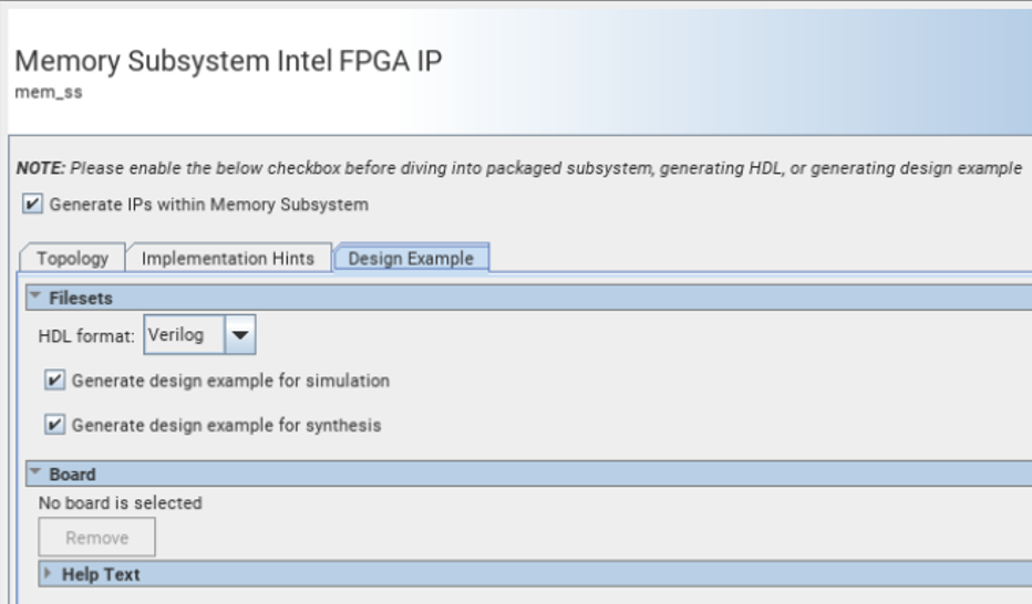
The Design Example tab provides the parameters to create a design example of the memory subsystem using your customized IP variant.
You can specify to create files for synthesis and simulation. You can also specify a target development board, if desired.
Figure 80. Design Example Tab
Generating a Design Example
- Set the appropriate parameters on the various tabs, for the memory subsystem IP that you want to create.
- Click the Generate Example Design button to generate a design example of the memory subsystem IP that you have configured.