Visible to Intel only — GUID: upx1665758713255
Ixiasoft
1. About the Agilex™ 7 F-Series and I-Series FPGA Memory Subsystem IP
2. Introduction to Memory Subsystem IP
3. Memory Subsystem IP Architecture and Feature Description
4. Memory Subsystem Features
5. Memory Subsystem Interfaces and Signals
6. Memory Subsystem User Operations
7. Memory Subsystem Register Descriptions
8. Parameterizing the Memory Subsystem IP
9. Simulating a Design Example
10. Document Revision History for Agilex™ 7 F-Series and I-Series FPGA Memory Subsystem IP User Guide
5.3.1. TCAM AXI-ST Request Interface
5.3.2. TCAM AXI-ST Response Interface
5.3.3. TCAM AXI-Lite Interface
5.3.4. BCAM AXI-ST Request Interface
5.3.5. BCAM AXI-ST Response Interface
5.3.6. BCAM AXI-Lite Interface
5.3.7. MBL AXI-ST Request Interface
5.3.8. MBL AXI-ST Response Interface
5.3.9. MBL AXI-Lite Interface
6.4.1. MBL Flush Operation
6.4.2. MBL Insert Key Operation
6.4.3. MBL Delete Key Operation
6.4.4. MBL Lookup Operation Using Key
6.4.5. MBL Modify Operation
6.4.6. MBL Modify Result Using Handle Operation
6.4.7. MBL Delete Key Using Handle Operation
6.4.8. MBL Lookup Using Handle Operation
6.4.9. MBL Insert Key if Not Present or Modify Result if Present Operation
6.4.10. MBL Get Handle Operation
7.2.1. Offset 0x0000 Version
7.2.2. Offset 0x0004 Feature List
7.2.3. Offset 0x0010 Memory Interfaces 0-7
7.2.4. Offset 0x0014 Memory Interfaces 8-15
7.2.5. Offset 0x0018 Memory Interfaces 16-23
7.2.6. Offset 0x001C Memory Interfaces 24-31
7.2.7. Offset 0x0020 Scratch Pad
7.2.8. Offset 0x0030 Control Policy (Lower DWORD)
7.2.9. Offset 0x0034 Control Policy (Upper DWORD)
7.2.10. Offset 0x0038 Read Access Control Policy (Lower DWORD)
7.2.11. Offset 0x003C Read Access Control Policy (Upper DWORD)
7.2.12. Offset 0x0040 Write Access Control Policy (Lower DWORD)
7.2.13. Offset 0x0044 Write Access Control Policy (Upper DWORD)
7.2.14. Offset 0x0050 Memory Status Bitmask 0
7.2.15. Offset 0x0054 Memory Status Bitmask 1
7.2.16. Offset 0x0058 Memory Ready Status 0
7.2.17. Offset 0x005C Memory Ready Status 1
7.2.18. Offset 0x0060 Memory Error Status 0
7.2.19. Offset 0x0064 Memory Error Status 1
7.3.2.1. Version
7.3.2.2. Feature List
7.3.2.3. Interface Attribute Parameters
7.3.2.4. Interface Attribute Parameters 1
7.3.2.5. Scratch Pad
7.3.2.6. General Control (GEN_CTRL)
7.3.2.7. Management Control (MGMT_CTRL)
7.3.2.8. Hash function_0 seed
7.3.2.9. Hash function_1 seed
7.3.2.10. Hash function_2 seed
7.3.2.11. Warning 0 (WARNING_0)
7.3.2.12. Fatal Error (FATAL_ERROR_0)
7.3.2.13. Monitor 0 (MON_)
7.3.2.14. Total Entries (TOTAL_ENTRIES)
7.3.2.15. Max. Rehouse Iterations (Max_Rehouse_Iterations)
7.3.2.16. Statistics Control (STATS_CTRL)
7.3.2.17. Active Table Entries (TABLE_ENTRIES)
7.3.2.18. Key_N
7.3.2.19. Result_N
7.5.1. MBL DFH
7.5.2. General MBL Registers
7.5.3. Version
7.5.4. Mbl_scratch
7.5.5. Mbl_gen_ctrl
7.5.6. Mbl_mgmt_ctrl
7.5.7. Mbl_key_handle
7.5.8. Mbl_nxt_handle_req
7.5.9. Mbl_nxt_handle
7.5.10. Mbl_warning_0
7.5.11. Mbl_fatal_0
7.5.12. Mbl_mon_0
7.5.13. Mbl_total_entries
7.5.14. Mbl_total_rehashes
7.5.15. Mbl_max_used_bins
7.5.16. Mbl_stats_ctrl
7.5.17. Mbl_stats_result
7.5.18. Mbl_max_lkup_latency
7.5.19. Mbl_max_rehash_index
7.5.20. Mbl_key
7.5.21. Mbl_res
8.2.5.1. Parameterizing the External Memory Interface (EMIF) IP
8.2.5.2. Parameterizing the Memory-Specific Adapter
8.2.5.3. Parameterizing the Content-Addressable Memory (CAM) IP
8.2.5.4. Parameterizing the External Memory Interfaces Calibration IP
8.2.5.5. Saving the IPs Within the Memory Subsystem
8.2.5.6. Propagation of Changes Across IPs within the Memory Subsystem IP
Visible to Intel only — GUID: upx1665758713255
Ixiasoft
3. Memory Subsystem IP Architecture and Feature Description
The memory subsystem IP includes a configurable, hardened protocol stack for external memory interfaces that allows you to configure from 1 to 8 EMIF instances, all implemented based on Agilex™ 7 EMIF IP core designs. The goal of the memory subsystem is to provide efficient ways to instantiate EMIF designs and provide application-level optimizations.
Memory subsystem build flow automatically identifies and connects subsystem internal building blocks to form the base subsystem and likewise for extended/vertical subsystem. For example, a memory base subsystem would automatically identify and connect the specific calibration block to the external memory instance(s) according to your specified subsystem placement of the physical external memory instance(s). The subsystem infrastructure comprises foundational IPs and standard protocol busses over an AXI interface.
The following figure shows the subsystem IP block diagram, with important blocks and their connections:
Figure 4. Memory Subsystem IP Block Diagram
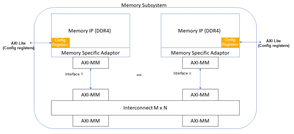
Each memory subsystem can contain single or multiple instances of memory IPs. You can connect subsystems with multiple IPs through the Platform Designer Interconnect. The subsystems can contain 0 or more lookup IPs and single or multiple user interfaces (AXI-MM). Each interface has dedicated clock and reset domains.
Although each usage has unique requirements, the subsystems share scalability, composeability, and a certain degree of infrastructure.