Visible to Intel only — GUID: amp1490746719612
Ixiasoft
Product Discontinuance Notification
1. About the RapidIO Intel FPGA IP Core
2. Getting Started
3. Parameter Settings
4. Functional Description
5. Signals
6. Software Interface
7. Testbench
8. Platform Designer (Standard) Design Example
9. RapidIO Intel FPGA IP User Guide Archives
10. Document Revision History for the RapidIO Intel® FPGA IP User Guide
A. Initialization Sequence
B. Porting a RapidIO Design from the Previous Version of Software
2.1. Installing and Licensing Intel® FPGA IP Cores
2.2. Generating IP Cores
2.3. IP Core Generation Output ( Intel® Quartus® Prime Standard Edition)
2.4. RapidIO IP Core Testbench Files
2.5. Simulating IP Cores
2.6. Integrating Your IP Core in Your Design
2.7. Specifying Timing Constraints
2.8. Compiling the Full Design and Programming the FPGA
2.9. Instantiating Multiple RapidIO IP Cores
2.6.1. Calibration Clock
2.6.2. Dynamic Transceiver Reconfiguration Controller
2.6.3. Transceiver Settings
2.6.4. Adding Transceiver Analog Settings for Arria II GX, Arria II GZ, and Stratix IV GX Variations
2.6.5. External Transceiver PLL
2.6.6. Transceiver PHY Reset Controller for Intel® Arria® 10 and Intel® Cyclone® 10 GX Variations
2.9.1. Clock and Signal Requirements for Arria® V, Cyclone® V, and Stratix® V Variations
2.9.2. Clock and Signal Requirements for Arria II GX, Arria II GZ, Cyclone IV GX, and Stratix IV GX Variations
2.9.3. Correcting the Synopsys Design Constraints File to Distinguish RapidIO IP Core Instances
2.9.4. Sourcing Multiple Tcl Scripts for Variations other than Intel® Arria® 10 and Intel® Cyclone® 10 GX
6.2.1. Capability Registers (CARs)
6.2.2. Command and Status Registers (CSRs)
6.2.3. Maintenance Interrupt Control Registers
6.2.4. Receive Maintenance Registers
6.2.5. Transmit Maintenance Registers
6.2.6. Transmit Port-Write Registers
6.2.7. Receive Port-Write Registers
6.2.8. Input/Output Master Address Mapping Registers
6.2.9. Input/Output Slave Mapping Registers
6.2.10. Input/Output Slave Interrupts
6.2.11. Transport Layer Feature Register
6.2.12. Error Management Registers
6.2.13. Doorbell Message Registers
7.1. Reset, Initialization, and Configuration
7.2. Maintenance Write and Read Transactions
7.3. SWRITE Transactions
7.4. NWRITE_R Transactions
7.5. NWRITE Transactions
7.6. NREAD Transactions
7.7. Doorbell Transactions
7.8. Doorbell and Write Transactions With Transaction Order Preservation
7.9. Port-Write Transactions
7.10. Transactions Across the Avalon® -ST Pass-Through Interface
Visible to Intel only — GUID: amp1490746719612
Ixiasoft
8.2.3.2. Connecting System Components
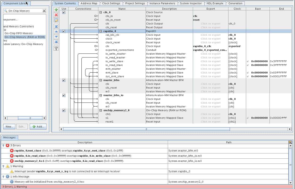
In Platform Designer (Standard), clicking and hovering the mouse over the Connections column displays the potential connection points between components, represented as dots connecting wires. A filled dot shows that a connection is made; an open dot shows a potential connection point that is not currently connected. Clicking a dot toggles the connection status. To complete this design, create the connections below.
| Make Connection From | To |
|---|---|
| clk_0 clk_reset | rapidio_0 clock_reset |
| master_bfm clk_reset | |
| master_bfm_io clk_reset | |
| onchip_mem... reset1 | |
| rapidio_0 mnt_master | rapidio_0 sys_mnt_slave |
| rapidio_0 io_read_master | onchip_mem... s1 |
| rapidio_0 io_write_master | onchip_mem... s1 |
| master_bfm m0 | rapidio_0 mnt_slave |
| rapidio_0 sys_mnt_slave | |
| master_bfm_io m0 | rapidio_0 io_write_slave |
| rapidio_0 io_read_slave | |
| onchip_mem... s1 |
Figure 43. Complete System Connections


Note: As described in Reset for RapidIO IP Cores, the circuitry necessary to ensure the correct behavior of the reset_n input signal to the RapidIO IP core is created automatically by Platform Designer (Standard). For this design example, you do not implement the logic described in the above figure , because Platform Designer (Standard) implements it for you.
The remaining errors are resolved as you modify the slave port base addresses, as described in the following section.
Related Information