Visible to Intel only — GUID: wyk1490746719940
Ixiasoft
Product Discontinuance Notification
1. About the RapidIO Intel FPGA IP Core
2. Getting Started
3. Parameter Settings
4. Functional Description
5. Signals
6. Software Interface
7. Testbench
8. Platform Designer (Standard) Design Example
9. RapidIO Intel FPGA IP User Guide Archives
10. Document Revision History for the RapidIO Intel® FPGA IP User Guide
A. Initialization Sequence
B. Porting a RapidIO Design from the Previous Version of Software
2.1. Installing and Licensing Intel® FPGA IP Cores
2.2. Generating IP Cores
2.3. IP Core Generation Output ( Intel® Quartus® Prime Standard Edition)
2.4. RapidIO IP Core Testbench Files
2.5. Simulating IP Cores
2.6. Integrating Your IP Core in Your Design
2.7. Specifying Timing Constraints
2.8. Compiling the Full Design and Programming the FPGA
2.9. Instantiating Multiple RapidIO IP Cores
2.6.1. Calibration Clock
2.6.2. Dynamic Transceiver Reconfiguration Controller
2.6.3. Transceiver Settings
2.6.4. Adding Transceiver Analog Settings for Arria II GX, Arria II GZ, and Stratix IV GX Variations
2.6.5. External Transceiver PLL
2.6.6. Transceiver PHY Reset Controller for Intel® Arria® 10 and Intel® Cyclone® 10 GX Variations
2.9.1. Clock and Signal Requirements for Arria® V, Cyclone® V, and Stratix® V Variations
2.9.2. Clock and Signal Requirements for Arria II GX, Arria II GZ, Cyclone IV GX, and Stratix IV GX Variations
2.9.3. Correcting the Synopsys Design Constraints File to Distinguish RapidIO IP Core Instances
2.9.4. Sourcing Multiple Tcl Scripts for Variations other than Intel® Arria® 10 and Intel® Cyclone® 10 GX
6.2.1. Capability Registers (CARs)
6.2.2. Command and Status Registers (CSRs)
6.2.3. Maintenance Interrupt Control Registers
6.2.4. Receive Maintenance Registers
6.2.5. Transmit Maintenance Registers
6.2.6. Transmit Port-Write Registers
6.2.7. Receive Port-Write Registers
6.2.8. Input/Output Master Address Mapping Registers
6.2.9. Input/Output Slave Mapping Registers
6.2.10. Input/Output Slave Interrupts
6.2.11. Transport Layer Feature Register
6.2.12. Error Management Registers
6.2.13. Doorbell Message Registers
7.1. Reset, Initialization, and Configuration
7.2. Maintenance Write and Read Transactions
7.3. SWRITE Transactions
7.4. NWRITE_R Transactions
7.5. NWRITE Transactions
7.6. NREAD Transactions
7.7. Doorbell Transactions
7.8. Doorbell and Write Transactions With Transaction Order Preservation
7.9. Port-Write Transactions
7.10. Transactions Across the Avalon® -ST Pass-Through Interface
Visible to Intel only — GUID: wyk1490746719940
Ixiasoft
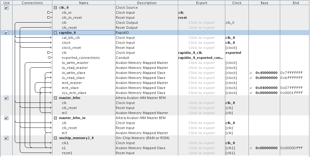
8.2.3.3. Assigning Addresses and Setting the Clock Frequency
To assign a specific address, follow these steps:
- Click on the address that you want to change in the Base column, then type the address that you want to assign. Make the following address assignments.
Table 132. Assign Addresses Port Name Base Address rapidio_0 io_write_slave 0x40000000 rapidio_0 io_read_slave 0x80000000 rapidio_0 mnt_slave 0x04000000 rapidio_0 sys_mnt_slave 0x00000000 onchip_mem... s1 0x00000000 - On the File menu, click Save and type rio_sys to save the Platform Designer (Standard) system in the rio_sys.qsys file.
Figure 44. Complete Platform Designer (Standard) Example System