Visible to Intel only — GUID: gwe1567781099914
Ixiasoft
1. Getting Started
2. Development Kit Overview
3. Power Up the Development Kit
4. Board Test System (BTS)
5. Development Kit Hardware and Configuration
6. Document Revision History for Intel® Stratix® 10 DX FPGA Development Kit User Guide
A. Development Kit Components
B. Safety and Regulatory Information
C. Compliance and Conformity Information
A.1. Components Overview
A.2. Power, Thermal, and Mechanical Considerations
A.3. Clock Circuits
A.4. Memory Interface
A.5. PCIe Interface
A.6. UPI Interface
A.7. Transceiver Signals: PCIe and UPI Interface
A.8. SlimSAS Connector
A.9. QSFP Network Interface
A.10. I2C Interface
A.11. QSPI Flash Memory
Visible to Intel only — GUID: gwe1567781099914
Ixiasoft
A.2.3. Mechanical Requirements
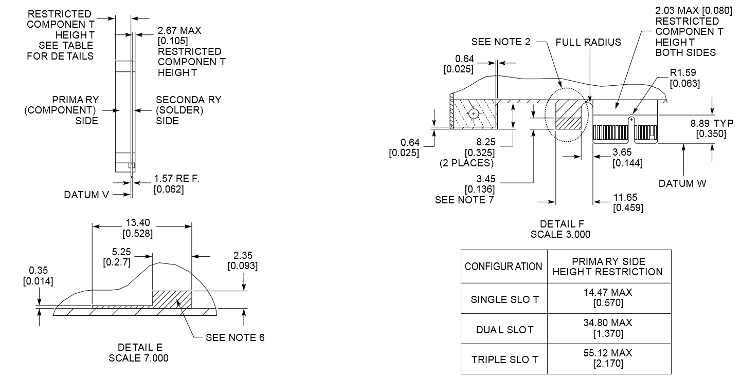
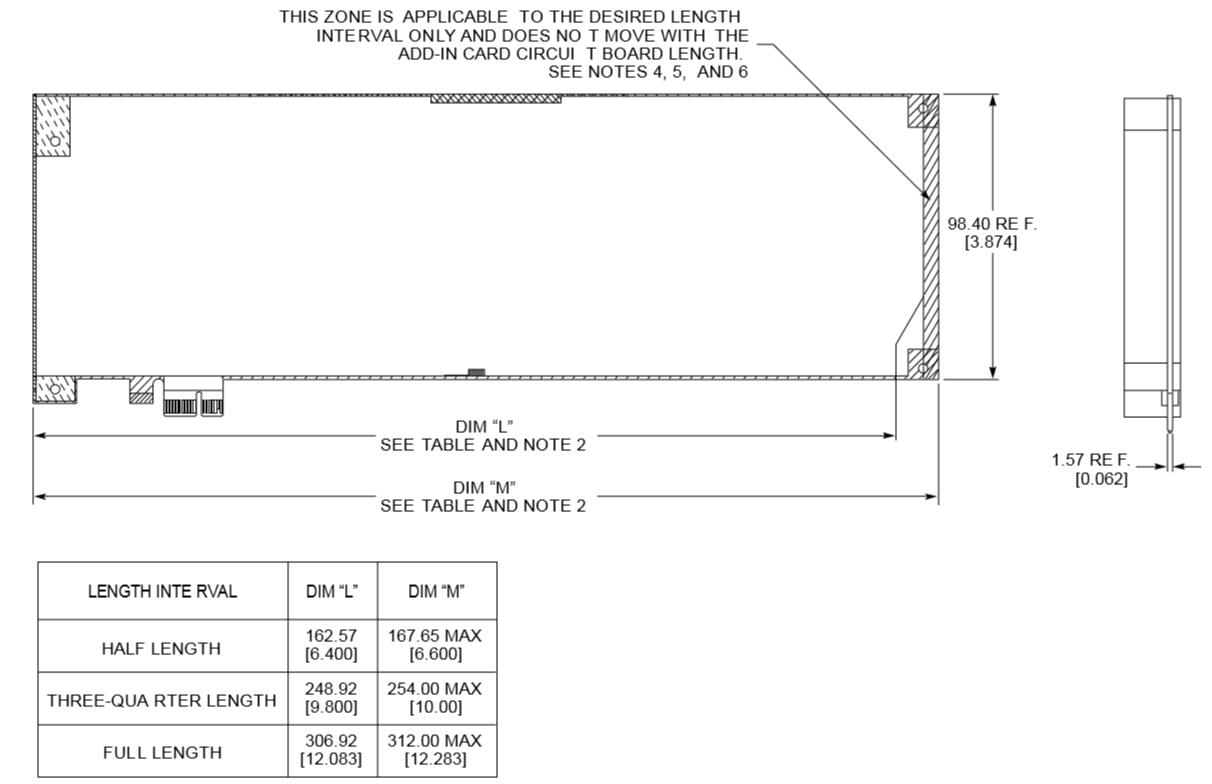
The Intel® Stratix® 10 DX FPGA Development Kit has a PCIe standard-height (4.376 in tall), 10.8” long, dual-slot (1.37 in high above the top surface of the PCB) form factor as defined by the PCIe CEM specification Revision 3.0. Additionally, this development kit includes the feature for retaining a high-mass card in the PCIe slot.
Figure 38. Sectional Profile


Figure 39. Top and Side Profile

