Visible to Intel only — GUID: dwn1574103485454
Ixiasoft
1. Getting Started
2. Development Kit Overview
3. Power Up the Development Kit
4. Board Test System (BTS)
5. Development Kit Hardware and Configuration
6. Document Revision History for Intel® Stratix® 10 DX FPGA Development Kit User Guide
A. Development Kit Components
B. Safety and Regulatory Information
C. Compliance and Conformity Information
A.1. Components Overview
A.2. Power, Thermal, and Mechanical Considerations
A.3. Clock Circuits
A.4. Memory Interface
A.5. PCIe Interface
A.6. UPI Interface
A.7. Transceiver Signals: PCIe and UPI Interface
A.8. SlimSAS Connector
A.9. QSFP Network Interface
A.10. I2C Interface
A.11. QSPI Flash Memory
Visible to Intel only — GUID: dwn1574103485454
Ixiasoft
4.3.5. Component DDR4 CH0 Tab
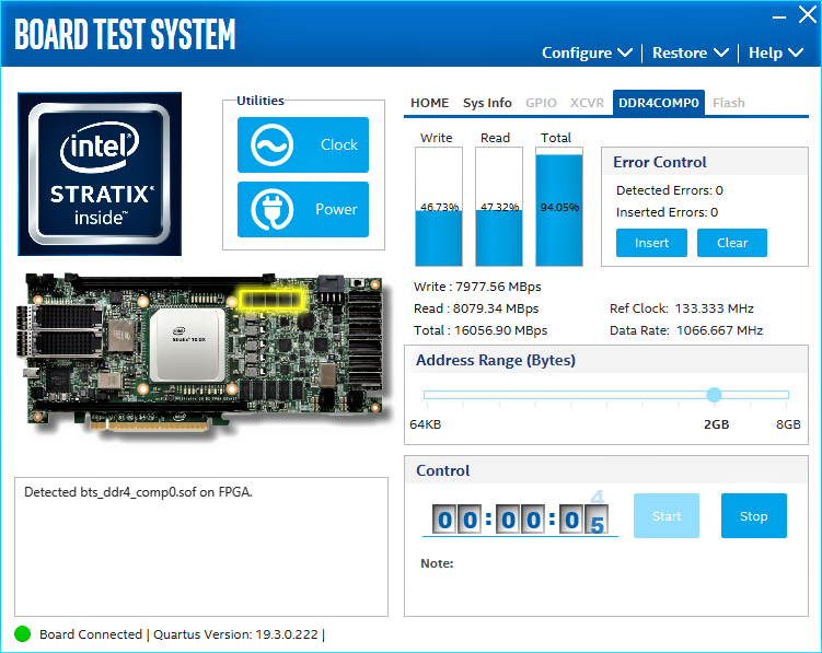
This tab allows you to read and write Component DDR4 CH0 memory on your board.
Figure 13. Component DDR4 CH0 Tab


The following sections describe the controls on the Component DDR4 CH0 tab:
Start
Initiates DDR4 memory transaction performance analysis.
Stop
Terminates transaction performance analysis.
Performance Indicator
These controls display current transaction performance analysis information collected since you last clicked Start:
- Write, Read and Total performance bars: Shows the percentage of maximum theoretical data rate that the requested transactions are able to achieve.
- Write (MBps), Read (MBps) and Total (MBps): Shows the number of bytes analyzed per second.
- Data Bus: 72-bits (8-bits ECC) wide and the frequency is 1066 MHz double data rate. 2133 Mbps per pin. Equating to a theoretical maximum banwidth of 136,512 Mbps or 17,064 MBps.
Error Control
This control displays data errors detected during analysis and allows you to insert errors:
- Detected errors: Displays the number of data errors detected in the hardware.
- Inserted errors: Displays the number of errors inserted into the transaction stream.
- Insert: Inserts a one-word error into the transaction stream each time you click the button. Insert error is only enabled during transaction performance analysis.
- Clear: Resets the detected error and inserted error counters to zero.
Address Range
Determines the number of addresses to use in each iteration of reads and writes.