Visible to Intel only — GUID: sgn1504827036364
Ixiasoft
4.2. Board Components
Figure 3. Board Picture (Top View)
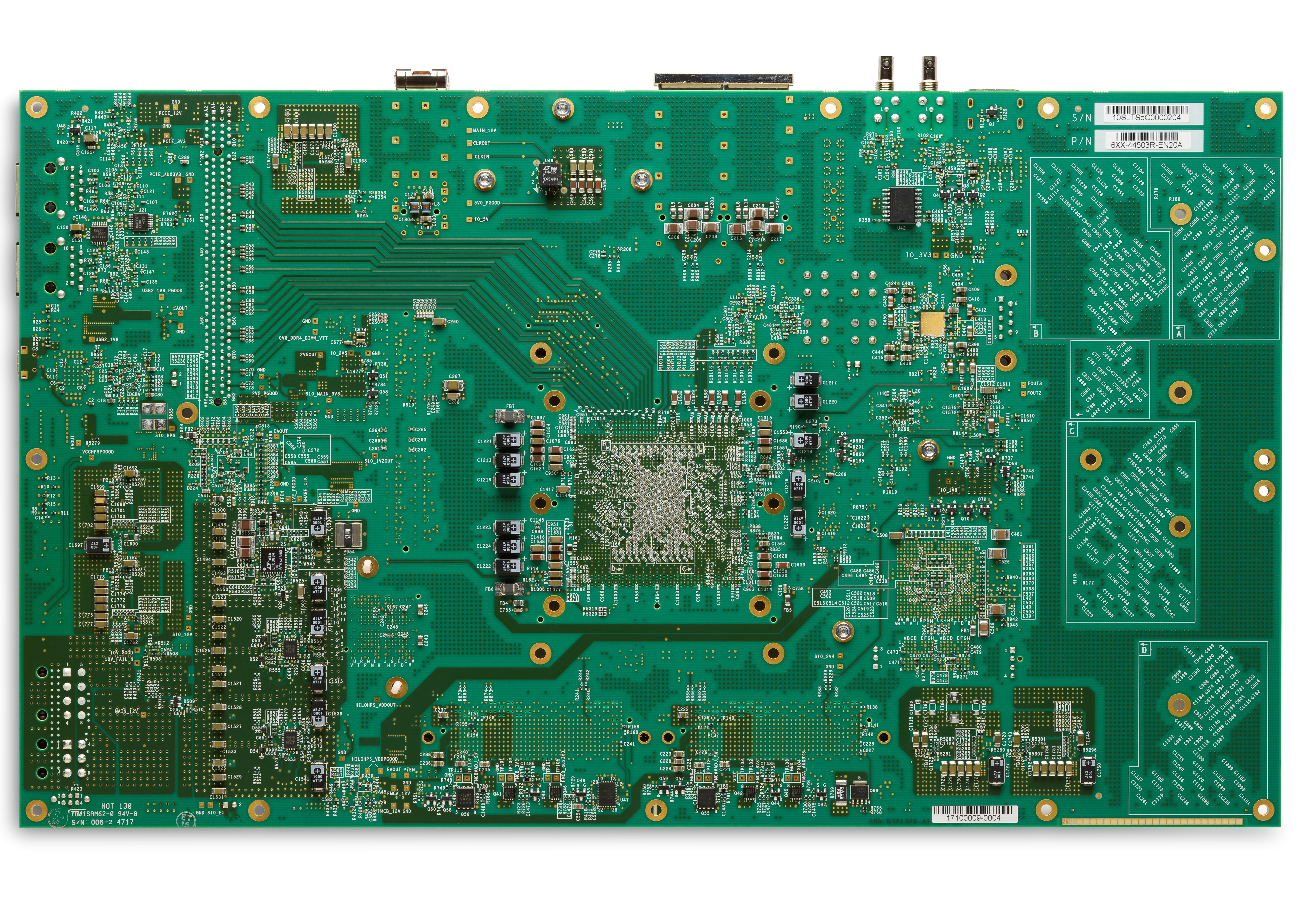
Figure 4. Board Picture (Bottom View)


Board Components Table
| Board Reference | Type | Description |
|---|---|---|
| Featured Device | ||
| U15 | FPGA | Stratix® 10 SoC FPGA |
| U43 | CPLD | MAX® 10 10M50DAF484I7G System Controller |
| U46 | CPLD | MAX® 10 10M16SAU169C8G Power Manager CPLD |
| Configuration, Status and Setup Elements | ||
| J1 | JTAG chain header | Provides access to the JTAG chain and disables the on-board Intel® FPGA Download Cable II when using an external JTAG debugger such as an Intel® FPGA Download Cable II |
| SW1 | JTAG chain control DIP switch | Remove or include devices in the active JTAG chain |
| SW2 | MSEL DIP Switch | Controls the configuration scheme on the board. MSEL pin 0,1,2 connect to the DIP Switch |
| J57 | Micro-USB Header | USB interface to on-board Intel® FPGA Download Cable II JTAG for programming and debugging HPS, FPGA or MAX® 10 CPLD through a type-B Micro-USB cable. |
| SW4 | Function DIP Switch | Selects I2C master, controls PCIe* slot power and selects FPGA image source |
| SW8 | Power Switch | ON position: Power GUI OFF position: Intel® Enpirion® dongle |
| S2 | Program select push button | Toggles the program select LEDs which selects the program image that loads from flash memory to the FPGA |
| S1 | Configure push button | Load image from flash memory to the FPGA based on the settings of the program select LEDs |
| D22 | Configuration done LED | Illuminates when the FPGA is configured |
| D20 | Load LED | Illuminates when the MAX® 10 CPLD System Controller |
| D19 | Error LED | Illuminates when the FPGA configuration from flash memory fails |
| D31 | Power LED | Illuminates when 3.3V power is present |
| D1, D2 | JTAG TX/RX LEDs | Indicates the transmit or receive activity of the JTAG chain. The TX and RX LEDs flicker if the link is in use and active. The LEDs are either off when not in use or on when in use but idle |
| D24, D26, D28 | Program select LEDs | Illuminates to show which flash memory image loads to the FPGA when you press the program select push button |
| D29, D30 | FMC port present LEDs | Illuminates when a daughtercard is plugged into the FMC port |
| Clock Circuits | ||
| U26 | Multi-output oscillator | Si5338A quad-output fixed oscillator with 148.5 MHz, 100 MHz, 27 MHz and 100 MHz outputs |
| U29 | 50-MHz oscillator | 50 MHz crystal oscillator for general purpose logic |
| U25 | Multi-output oscillator | Two 100 MHz outputs for PCIe* application |
| J19, J20 | Clock input SMA connector | External clock inputs for the transceiver test port |
| U33 | Multi-output oscillator | Si5341 ten-output fixed oscillator |
| U31 | Multi-output oscillator | Si5338A quad-output fixed oscillator with four 133.33 MHz outputs |
| U34 | Multi-output clock cleaner | LMK05028 Clock Cleaner |
| General User Input/Output | ||
| D21, D23, D25, D27 | User LEDs | Four user LEDs. Illuminate when driven high. |
| SW3 | User DIP Switch | User DIP switch. When the switch is ON, a logic 0 is selected |
| S3 | FPGA Reset Push Button | Reset the FPGA logic |
| S4, S5, S6, S7 | General user push buttons | Four user push buttons. Driven low when pressed |
| S20 | HPS Reset Push Buttons | HPS cold/warm reset push buttons |
| Memory Connectors | ||
| J13 | HPS HILO Memory Connector | HPS memory card include DDR3 HILO memory card and DDR4 HILO memory card |
| J14 | Boot Flash Connector | Boot flash card options include QSPI flash card, SD micro flash card |
| J28 | SO-DIMM | 16 GB SO-DIMM DDR4 Memory Card |
| U41 | I2C EEPROM | 32 Kb I2C serial EEPROM |
| Communication Ports | ||
| J53 | PCIe* socket | Gen3 x16 Socket |
| J11, J12 | FMC Port | J29 is a V57.4 compatible FMC connector. J19 is a FMC connector defined by Intel® 16 transceivers specification |
| J7 | SFP+ Port | One SFP+ Ports |
| J3 | Gigabit Ethernet Port | SGMII Gigabit Ethernet port through FPGA transceiver |
| J4 | Gigabit Ethernet Port | SGMII Gigabit Ethernet Port through FPGA transceiver |
| J9-J10 | QSFP28 Optical Transceiver Interface | 17 Gbps/28 Gbps, 8 channels connected to QSFP28 modules |
| J57, U2 | USB-UART Port | Mini-B USB interface to USB-to-UART bridge for serial UART interface |
| J22 | DB9 UART Port | DB9 RS-232 UART Port |
| U42 | Real-time clock | DS1339 device with built-in power sense circuit that detects power failures and automatically switches to backup battery supply, maintaining time keeping even when the board is not powered |
| Video and Display Ports | ||
| J8 | HDMI Port | Display Port interface |
| J5, U13 | SDI Video Output Port | HDBNC 75-Ohm SDI video TX interface |
| J6, U14 | SDI Video Input Port | HDBNC 75-Ohm SDI video RX interface |
| J29 | Power GUI Connector | Intel® Enpirion® Power GUI Connector |
| Power Supply | ||
| J25, J55 | DC input jack | Accepts 12 V DC power supply |
| SW7 | Power Switch | Switch to power on or off the board when power is supplied from the DC input jack |