Visible to Intel only — GUID: skj1682961658264
Ixiasoft
4.1. Identifying Pin Assignments Based on Byte Location
4.2. Assigning the RZQ pin and Dedicated Reference Clock Pin for MIPI D-PHY IP
4.3. Supported I/O Features in MIPI D-PHY I/O Standard
4.4. Using the Remaining I/O Pin from Same Byte Location
4.5. I/O Bank Sharing
4.6. MIPI D-PHY Placement Rules
4.7. MIPI Interface Layout Design Guidelines
4.8. Handling MIPI D-PHY IP Reset
6.2.1.1. IP_ID
6.2.1.2. IP_CAP
6.2.1.3. D0_CAP
6.2.1.4. DN_CAP
6.2.1.5. RX_CAP
6.2.1.6. TX_CAP
6.2.1.7. TX_PREAMBLE_LEN
6.2.1.8. D-PHY_CSR
6.2.1.9. TX_CLK_LANE_PS
6.2.1.10. RX_DLANE_ERR
6.2.1.11. SKEW_CAL_LEN_B0
6.2.1.12. SKEW_CAL_LEN_B1
6.2.1.13. SKEW_CAL_LEN_B2
6.2.1.14. SKEW_CAL_LEN_B3
6.2.1.15. ALT_CAL_LEN_B0
6.2.1.16. ALT_CAL_LEN_B1
6.2.1.17. ALT_CAL_LEN_B2
6.2.1.18. ALT_CAL_LEN_B3
6.2.1.19. CLK_CSR
6.2.1.20. CLK_STATUS
6.2.1.21. DLANE_CSR_0
6.2.1.22. DLANE_STATUS_0
6.2.1.23. RX_DLANE_DESKEW_DELAY_0
6.2.1.24. RX_DLANE_ERR_0
6.2.1.25. DLANE_CSR_1
6.2.1.26. DLANE_STATUS_1
6.2.1.27. RX_DLANE_DESKEW_DELAY_1
6.2.1.28. RX_DLANE_ERR_1
6.2.1.29. DLANE_CSR_2
6.2.1.30. DLANE_STATUS_2
6.2.1.31. RX_DLANE_DESKEW_DELAY_2
6.2.1.32. RX_DLANE_ERR_2
6.2.1.33. DLANE_CSR_3
6.2.1.34. DLANE_STATUS_3
6.2.1.35. RX_DLANE_DESKEW_DELAY_3
6.2.1.36. RX_DLANE_ERR_3
6.2.1.37. DLANE_CSR_4
6.2.1.38. DLANE_STATUS_4
6.2.1.39. RX_DLANE_DESKEW_DELAY_4
6.2.1.40. RX_DLANE_ERR_4
6.2.1.41. DLANE_CSR_5
6.2.1.42. DLANE_STATUS_5
6.2.1.43. RX_DLANE_DESKEW_DELAY_5
6.2.1.44. RX_DLANE_ERR_5
6.2.1.45. DLANE_CSR_6
6.2.1.46. DLANE_STATUS_6
6.2.1.47. RX_DLANE_DESKEW_DELAY_6
6.2.1.48. RX_DLANE_ERR_6
6.2.1.49. DLANE_CSR_7
6.2.1.50. DLANE_STATUS_7
6.2.1.51. RX_DLANE_DESKEW_DELAY_7
6.2.1.52. RX_DLANE_ERR_7
6.2.1.53. TX_LPX
6.2.1.54. TX_HS_EXIT
6.2.1.55. TX_LP_EXIT
6.2.1.56. TX_CLK_PREPARE
6.2.1.57. TX_CLK_ZERO
6.2.1.58. TX_CLK_POST
6.2.1.59. TX_CLK_PRE
6.2.1.60. TX_HS_PREPARE
6.2.1.61. TX_HS_ZERO
6.2.1.62. TX_HS_TRAIL
6.2.1.63. TX_INIT
6.2.1.64. TX_WAKE
6.2.1.65. RX_CLK_LOSS_DETECT
6.2.1.66. RX_CLK_SETTLE
6.2.1.67. RX_HS_SETTLE
6.2.1.68. RX_INIT
6.2.1.69. RX_CLK_POST
6.2.1.70. RX_CAL_REG_CTRL
6.2.1.71. RX_CAL_STATUS_D-PHY
6.2.1.72. RX_CAL_SKEW_W_START_MUX
6.2.1.73. RX_CAL_SKEW_W_END_MUX
6.2.1.74. RX_CAL_ALT_W_START_MUX
6.2.1.75. RX__CAL_ALT_W_END_MUX
6.2.1.76. RX_DESKEW_DELAY_MUX
6.2.1.77. RX_CAL_STATUS_LANE_MUX
6.2.1.78. PRBS_INIT_0
6.2.1.79. PRBS_INIT_1
6.2.1.80. PRBS_INIT_2
6.2.1.81. PRBS_INIT_3
6.2.1.82. PRBS_INIT_4
6.2.1.83. PRBS_INIT_5
6.2.1.84. PRBS_INIT_6
6.2.1.85. TX_TM_CONTROL
6.2.1.86. TX_MNL_IO_0
6.2.1.87. TX_MNL_D_LP_EN
6.2.1.88. RX_TM_CONTROL
6.2.2.1. TG_TOP_CTRL_0
6.2.2.2. TG_TOP_CTRL_1
6.2.2.3. TG_TOP_DONE
6.2.2.4. TG_TOP_FAIL
6.2.2.5. TG_TOP_TEST_EN
6.2.2.6. TG_TOP_TEST_LINK
6.2.2.7. TARGET_TEST_CNT
6.2.2.8. TCHK_CONTROL
6.2.2.9. TCHK_LINK_STATUS
6.2.2.10. HS_DONE_LANES
6.2.2.11. TCHK_LINK_ERR_STATUS
6.2.2.12. LANE_ERROR_SOT_LANES
6.2.2.13. CAL_ERROR_LANES
6.2.2.14. HS_ERR_LANES
6.2.2.15. HS_TEST_CNT
6.2.2.16. LPDT_TEST_CNT
6.2.2.17. TRIGGER_TEST_CNT
6.2.2.18. ULPS_TEST_CNT
6.2.2.19. TG_RX_OVRD_DATA_PAT
6.2.2.20. TG_RX_BIT_ERROR_CNT
6.2.2.21. TG_RX_HS_TXFER_CNT
6.2.2.22. TG_LINK_CONTROL
6.2.2.23. TG_INIT_CNT
6.2.2.24. TG_HS_LEN
6.2.2.25. TG_LP_LEN
6.2.2.26. TG_SKEW_CAL
6.2.2.27. TG_ALT_CAL
6.2.2.28. TG_PER_SKEW_CAL_LEN
6.2.2.29. TG_TEST_CNT
6.2.2.30. TG_OVRD_DATA_PAT
6.2.2.31. TG_TX_HS_TXFER_CNT
Visible to Intel only — GUID: skj1682961658264
Ixiasoft
3. Agilex™ 5 MIPI D-PHY Architecture
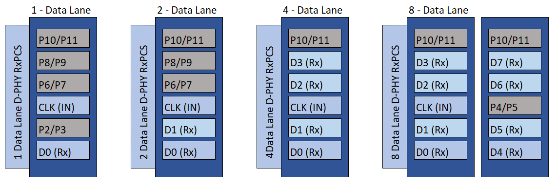
Agilex™ 5 supports MIPI D-PHY through HSIO banks. Each HSIO bank consists of 8 byte blocks to support MIPI D-PHY; however, one byte blocks is reserved for RZQ calibration and reference clock. Therefore the maximum MIPI D-PHY that a single HSIO bank can support is up to 7 interfaces (subject to D-PHY lanes configuration). The Agilex™ 5 D-PHY offers a native D-PHY interface that allows direct point-to-point connection between the D-PHY transmitter and D-PHY receiver without any passive circuitry or third-party component in between. Each interface can support 1, 2, 4, or 8 data lanes plus 1 clock lane.
Each interface has prefixed data lane and clock lane placement as illustrated in the diagram below. Refer to the MIPI D-PHY Interface Implementation section to understand the implementation and how to identify the physical pin placement.
Figure 2. Agilex™ 5 MIPI D-PHY TX Data and Clock Lane Placement
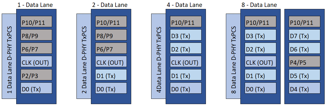
Figure 3. Agilex™ 5 MIPI D-PHY RX Data and Clock Lane Placement