6.1.4. D-PHY RX PPI Interface Signals
These PPI interface signals are used only when the D-PHY IP is configured for receive (RX). Each lane (clock and data) of each link has a PPI RX interface attached to it.
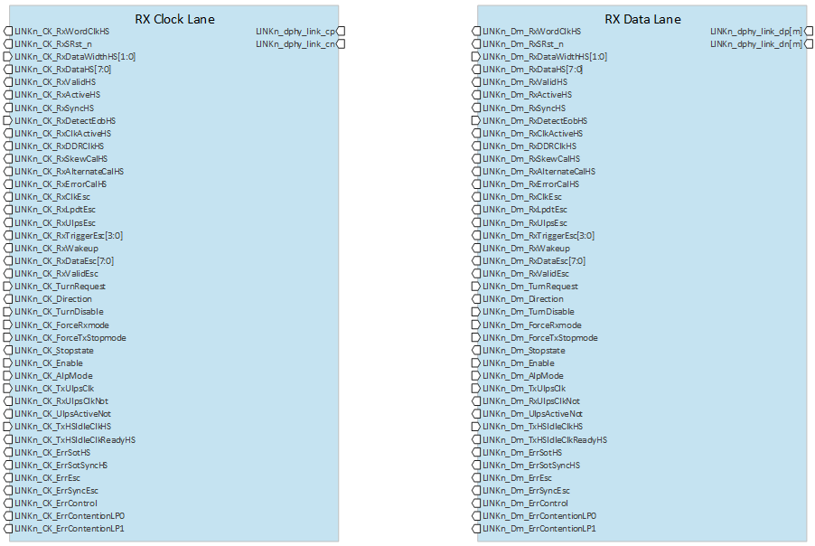
Figure 24. PPI Interface Signals
| Signal | Direction | Width | Description |
|---|---|---|---|
| High-Speed Receive Signals (Link n, Clock Lane) - RX only | |||
| LINKn_CK_RxWordClkHS | Output | 1 | High-Speed Receive Word Clock (link n, clock lane) This is used to synchronize signals in the high-speed receive clock domain. The RxWordClkHS is generated by dividing the recovered high-speed clock. The frequency of RxWordClkHS is dependent upon the width of the High-Speed Receive Data, as follows:
For links with multiple data Lanes, the PHY implements one RxWordClkHS signal per lane. |
| LINKn_CK_RxSRst_n | Output | 1 | Link Sync Reset (link n, clock lane). Link synchronous reset (synchronized to Linkn_CK_RxWordClkHS). |
| LINKn_CK_RxDataWidthHS | Input | 2 | High-Speed Receive Data Width Select (link n, clock lane). Selects the bus width of RxDataHS:
An implementation may support any data width - one fixed width, or subset of widths or all widths defined above. |
| LINKn_CK_RxDataHS | Output | 8 | High-Speed Receive Data (link n, clock lane). |
| LINKn_CK_RxValidHS | Output | 1 | High-Speed Receive Data Valid (link n, clock lane.) |
| LINKn_CK_RxActiveHS | Output | 1 | High-Speed Reception Active (link n, clock lane) This active high signal indicates that the Lane Module is actively receiving a High-Speed transmission from the Lane interconnect. There is no timing relationship between Stopstate being deasserted and RxActiveHS being asserted. Likewise, there is no relationship between Stopstate being asserted and RxActiveHS being deasserted. When receiving any high speed data transfer including Alternate Calibration or high speed deskew pattern, RxActiveHS is asserted. |
| LINKn_CK_RxSyncHS | Output | 1 | Receiver Synchronization Observed (link n, clock lane). |
| LINKn_CK_RxDetectEobHS | Input | 1 | Receiver Detection Of End Of Burst (link n, clock lane). |
| LINKn_CK_RxClkActiveHS | Output | 1 | Receiver Clock Active (link n, clock lane) This asynchronous, active high signal indicates that a Clock Lane is receiving a DDR Clock signal. There is no timing relationship between Stopstate being deasserted and RxClkActiveHS being asserted. Likewise, there is no relationship between Stopstate being asserted and RxClkActiveHS being deasserted. |
| LINKn_CK_RxDDRClkHS | Output | 1 | Receiver DDR Clock (link n, clock lane. |
| LINKn_CK_RxSkewCalHS | Output | 1 | High-Speed Receive Skew Calibration (link n, clock lane). |
| LINKn_CK_RxAlternateCalHS | Output | 1 | High-Speed Receive Alternate Calibration Sequence (link n, clock lane). |
| LINKn_CK_RxErrorCalHS | Output | 1 | High-Speed Receive Calibration Error (link n, clock lane) . |
| Escape Mode Receive Signals (Link n, Clock Lane) - RX only | |||
| LINKn_CK_RxClkEsc | Output | 1 | Escape Mode Receive Clock (link n, clock lane) This signal is used to transfer received data to the protocol during LP mode and ALP mode. In LP mode, this signal is generated from the two Low-Power signals in the Lane interconnect. Because of the asynchronous nature of Escape Mode data transmission, this signal may not be periodic. The number of pulses of this signal is limited to the activity on the lines, so it is advisable that this signal not be used as clock for the protocol layer. In ALP mode, this clock is generated by dividing the recovered high-speed clock, and is exactly 1/8 the high-speed received data rate. |
| LINKn_CK_RxLpdtEsc | Output | 1 | Escape Low-Power Data Receive mode (link n, clock lane). |
| LINKn_CK_RxUlpsEsc | Output | 1 | Escape Ultra-Low Power (Receive) mode (link n, clock lane) This active high signal is asserted to indicate that the Lane Module has entered the Ultra-Low Power State, due to the detection of a received ULPS command. The Lane Module remains in this mode with RxUlpsEsc asserted until a Stop state is detected on the Lane interconnect. |
| LINKn_CK_RxTriggerEsc | Output | 4 | Escape Mode Receive Trigger 0-3 (link n, clock lane). |
| LINKn_CK_RxWakeup | Output | 1 | Receiver Wakeup Pulse Detected (link n, clock lane) For ALP mode implementations, this active high signal indicates that a wakeup pulse (ALP-01) is currently being detected. This signal is driven directly from the analog ALP wakeup detector and is not timed to any PPI signal. |
| LINKn_CK_RxDataEsc | Output | 8 | Escape Mode Receive Data (link n, clock lane). |
| LINKn_CK_RxValidEsc | Output | 1 | Escape Mode Receive Data Valid (link n, clock lane). |
| Control Signals (Link n, Clock Lane) | |||
| LINKn_CK_TurnRequest | Input | 1 | Turnaround Request (link n, clock lane). |
| LINKn_CK_Direction | Output | 1 | Transmit/Receive Direction (link n, clock lane) This signal is used to indicate the current direction of the Lane interconnect.
Any abnormalities during the BTA procedure can result in contention conditions, requiring the protocol layer to implement mechanisms to detect and resolve. |
| LINKn_CK_TurnDisable | Input | 1 | Disable Turnaround (link n, clock lane). |
| LINKn_CK_ForceRxmode | Input | 1 | Force Lane Module Into Receive mode / Wait for Stop state (link n, clock lane) - RX only This signal allows the protocol to initialize a Lane Module, or force a Bi-directional Lane Module, into receive mode. This signal is used during initialization or to resolve a contention situation. When this signal is high, the Lane Module immediately transitions into receive Control mode and waits for a Stop state to appear on the Lane interconnect. When used for initialization, this signal will be released (i.e., driven low) only when the Dp Dn inputs are in Stop state for a time TINIT, or longer. The assertion of ForceRxmode and ForceTxStopmode are mutually exclusive. |
| LINKn_CK_ForceTxStopmode | Input | 1 | Force Lane Module Into Transmit mode / Generate Stop state (link n, clock lane) - TX only This signal allows the protocol to force a Lane Module into transmit mode and Stop state during initialization or following an error situation, e.g. expired time out. When this signal is high, the Lane Module immediately transitions into transmit mode and the module state machine is forced into the Stop state. The protocol layer does not assert TxRequestEsc, TxRequestHS, or Turnrequest for an implementation-specific period of time after the deassertion of ForceTxStopMode, in order to create a safe margin for the PHY to be able to accept a new request. The assertion of ForceRxmode and ForceTxStopmode are mutually exclusive. |
| LINKn_CK_Stopstate | Output | 1 | Lane is in Stop state (link n, clock lane) This active high signal indicates that the Lane Module, regardless of whether the Lane Module is a transmitter or a receiver, is currently in Stop state. This indicates that the PHY Line levels are in the LP-11 state, and the PHY state machine is in the stop state and ready to receive a request for the next operation. Also, the protocol may use this signal to indirectly determine if the PHY Line levels are in the LP-11 state. A Master will not assert this signal during initialization until after LP-11 has been driven for the required TINIT time. A Slave will not assert this signal during initialization until after LP-11 has been detected for the required TINIT time. |
| LINKn_CK_Enable | Input | 1 | Enable Lane Module (link n, clock lane) This active high signal forces the Lane Module out of “shutdown”. All Line drivers, receivers, terminators, and contention detectors are turned off when Enable is low. Furthermore, while Enable is low, all other PPI inputs are ignored, and all PPI outputs are driven to the default inactive state. Enable is a level sensitive signal and does not depend on any clock. |
| LINKn_CK_AlpMode | Input | 1 | Alternate Low Power Mode Selection (link n, clock lane). |
| LINKn_CK_TxUlpsClk | Input | 1 | Transmit Ultra-Low Power State on Clock Lane (link n, clock lane) - TX only This active-high signal is asserted to cause a Clock Lane Module to enter the Ultra-Low Power State. The Lane Module remains in this mode until TxUlpsClk is de-asserted. |
| LINKn_CK_RxUlpsClkNot | Output | 1 | Receive Ultra-Low Power State on Clock Lane (link n, clock lane) - RX only This active low signal is asserted to indicate that the Clock Lane Module has entered the Ultra-Low Power State due to the detection of a request to enter the ULP state. The Lane Module remains in this mode with RxUlpsClkNot asserted until a Stop state is detected on the Lane Interconnect. |
| LINKn_CK_UlpsActiveNot | Output | 1 | ULP State (not) Active (link n, clock lane) This active low signal is asserted to indicate that the Lane is in ULP state. For a transmitter, this signal is asserted some time after TxUlpsEsc and TxRequestEsc (TxUlpsClk for a Clock Lane) are asserted. The transmitting PHY continues to supply TxClkEsc until UlpsActiveNot is asserted. To leave ULP state, the transmitter first drives TxUlpsExit high, then waits for UlpsActiveNot to become high (inactive). At that point, the transmitting PHY is active and has started transmitting a Mark-1 on the Lines. The protocol waits for a time Twakeup and then drives TxRequestEsc (TxUlpsClk) inactive to return the Lane to Stop state. For a receiver, this signal indicates that the Lane is in ULP state. When entering the ULP state, RxUlpsEsc (or RxUlpsClkNot for a Clock Lane) is asserted to indicate the detection of the ULPS command and entry into the ULP state, followed by the assertion of the UlpsActiveNot, indicating that the PHY is in the ULP state. When exiting the ULP state, this signal is deasserted to indicate that the PHY has detected a Mark-1 to initiate the exit from the ULP state. After the required TWAKEUP, the RxUlpsEsc, or RxUlpsClkNot for a Clock Lane, is deasserted to indicate the PHY has exited the ULP state and LP-11 has been detected. |
| LINKn_CK_TxHSIdleClkHS | Input | 1 | HS-Idle State Start (link n, clock lane). |
| LINKn_CK_TxHSIdleClkReadyHS | Output | 1 | Clock Ready to Exit HS-Idle-ClkHS0 Sub-State (link n, clock lane). |
| Error Signals (Link n, Clock Lane) - RX only | |||
| LINKn_CK_ErrSotHS | Output | 1 | Start-of-Transmission (SoT) Error (link n, clock lane). |
| LINKn_CK_ErrSotSyncHS | Output | 1 | Start-of-Transmission Synchronization Error (link n, clock lane). |
| LINKn_CK_ErrEsc | Output | 1 | Escape Entry Error (link n, clock lane). |
| LINKn_CK_ErrSyncEsc | Output | 1 | Low-Power Data Transmission Synchronization Error (link n, clock lane). |
| LINKn_CK_ErrControl | Output | 1 | Control Error (link n, clock lane) This active high signal is asserted when an incorrect Line state sequence is detected in LP and ALP modes. Once asserted, this signal remains asserted until the next transaction starts, so that the protocol can properly process the error. Section A.18 describes the LP and ALP signaling error sequences that require this signal to be asserted, as well as error sequences that can optionally result in this signal being asserted. Sequences that can optionally result in this signal being asserted are implementation specific. |
| LINKn_CK_ErrContentionLP0 | Output | 1 | LP0 Contention Error (link n, clock lane). |
| LINKn_CK_ErrContentionLP1 | Output | 1 | LP1 Contention Error (link n, clock lane). |
| Signal | Direction | Width | Description |
|---|---|---|---|
| High-Speed Receive Signals (Link n, Data Lane m) - RX only | |||
| LINKn_Dm_RxWordClkHS | Output | 1 | High-Speed Receive Word Clock (link n, data lane m) This signal synchronizes signals in the high-speed receive clock domain. The RxWordClkHS is generated by dividing the recovered high-speed clock. The frequency of RxWordClkHS is dependent upon the width of the High-Speed Receive Data, as follows:
For links with multiple data Lanes, the PHY implements one RxWordClkHS signal per lane. |
| LINKn_Dm_RxSRst_n | Output | 1 | Link Sync Reset (link n, data lane m) Link synchronous reset (synchronized to Linkn_CK_RxWordClkHS). |
| LINKn_Dm_RxDataWidthHS | Input | 2 | High-Speed Receive Data Width Select (link n, data lane m) Selects the bus width of RxDataHS:
An implementation may support any data width - one fixed width, or subset of widths or all widths defined above. |
| LINKn_Dm_RxDataHS | Output | 8 | High-Speed Receive Data (link n, data lane m) High-speed data received by the Lane Module. If the RxValidHS signals indicate that more than 8 bits were received, then the byte reception order over the physical interface is: RxDataHS[7:0] followed by RxDataHS[15:8] followed by RxDataHS[23:16] followed by RxDataHS[31:24]. Data is transferred on rising edges of RxWordClkHS. The following signals are defined for the High-Speed Receive Data based on the width of the receive data path:
An implementation may support any data width - one fixed width, or subset of widths or all widths defined above. The LSB will be received as the first bit and the MSB will be received as the last bit. |
| LINKn_Dm_RxValidHS | Output | 1 | High-Speed Receive Data Valid (link n, data lane m) This active high signal indicates that the Lane Module is driving data to the protocol layer on the RxDataHS output. There is no “RxReadyHS” signal, and the protocol layer is expected to capture RxDataHS on every rising edge of RxWordClkHS where any RxValidHS bit is asserted. There is no provision for the protocol layer to slow down (“throttle”) the receive data. The following High-Speed Receive Data Valid signals are defined based on the width of the receive data path:
The following High-Speed Receive Data Valid signals indicate which bits of the RxDataHS data bus contain valid data as follows:
For links with more than one data Lane, it is possible that each data Lane’s RxValidHS low-to-high and high-to-low transition may be in a different RxWordClkHS cycle. RxValidHS is not asserted for high speed deskew bursts or alternate calibration sequences. RxValidHS is not asserted if ErrSotSyncHS is asserted. If the PHY does not support EOT processing, all bits of RxValidHS[0], RxValidHS[1:0], or RxValjdHS[3:0] are asserted when there is valid data received from the channel. |
| LINKn_Dm_RxActiveHS | Output | 1 | High-Speed Reception Active (link n, data lane m) This active high signal indicates that the Lane Module is actively receiving a High-Speed transmission from the Lane interconnect. There is no timing relationship between Stopstate being deasserted and RxActiveHS being asserted. Likewise, there is no relationship between Stopstate being asserted and RxActiveHS being deasserted. When receiving any high speed data transfer including Alternate Calibration or high speed deskew pattern, RxActiveHS is asserted. |
| LINKn_Dm_RxSyncHS | Output | 1 | Receiver Synchronization Observed (link n, data lane m) This active-high signal indicates that the Lane Module has seen an appropriate synchronization event. In a typical High-Speed transmission, RxSyncHS is high for one cycle of RxWordClkHS at the beginning of a High-Speed transmission when RxActiveHS is first asserted. RxSyncHS is asserted even if ErrSotHS is asserted. RxSyncHS is not asserted if ErrSotSyncHS is asserted. |
| LINKn_Dm_RxDetectEobHS | Input | 1 | Receiver Detection Of End Of Burst (link n, data lane m). |
| LINKn_Dm_RxClkActiveHS | Output | 1 | Receiver Clock Active (link n, data lane m) This asynchronous, active high signal indicates that a Clock Lane is receiving a DDR Clock signal. There is no timing relationship between Stopstate being deasserted and RxClkActiveHS being asserted. Likewise, there is no relationship between Stopstate being asserted and RxClkActiveHS being deasserted. |
| LINKn_Dm_RxDDRClkHS | Output | 1 | Receiver DDR Clock (link n, data lane m). |
| LINKn_Dm_RxSkewCalHS | Output | 1 | High-Speed Receive Skew Calibration (link n, data lane m) This optional active-high signal indicates that the high speed deskew burst is being received. RxSkewCalHS is set to the active state when the all-ones sync pattern is received, and is cleared to the inactive state when Dp and Dn transition back to the LP-11 Stop State. RxSkewCalHS is not asserted for the Alternate Calibration Sequence. |
| LINKn_Dm_RxAlternateCalHS | Output | 1 | High-Speed Receive Alternate Calibration Sequence (link n, data lane m) This optional active-high signal indicates that the alternate Calibration Sequence is being received. RxAlternateCalHS is set to the active state when the “11110000” sync pattern is received, and is cleared to the inactive state when Dp and Dn transition back to the LP-11 Stop State. |
| LINKn_Dm_RxErrorCalHS | Output | 1 | High-Speed Receive Calibration Error (link n, data lane m) This optional asynchronous active-high signal indicates that the high speed calibration ended with errors. This signal is asserted if the initial deskew calibration (RxSkewCalHS is asserted) or alternate calibration (RxAlternateCalHS is asserted) has not completed successfully. If it is asserted in any of the initial calibrations, proper received data cannot be expected, and the system takes an implementation-specific action to resolve the condition. This signal can also be asserted if periodic deskew (RxSkewCalHS is asserted) or preamble sequence did not complete successfully. It is implementation-specific how the system responds to this condition. RxErrorCalHS signal continues to be asserted until a new calibration sequence is received, or the PHY is disabled and re-enabled. |
| Escape Mode Receive Signals (Link n, Data Lane m) - RX only | |||
| LINKn_Dm_RxClkEsc | Output | 1 | Escape Mode Receive Clock (link n, data lane m) This signal transfers received data to the protocol during LP mode and ALP mode. In LP mode, this signal is generated from the two Low-Power signals in the Lane interconnect. Because of the asynchronous nature of Escape Mode data transmission, this signal may not be periodic. The number of pulses of this signal is limited to the activity on the lines, so it is advisable that this signal not be used as clock for the protocol layer. In ALP mode, this clock is generated by dividing the recovered high-speed clock, and is exactly 1/8 the high-speed received data rate. |
| LINKn_Dm_RxLpdtEsc | Output | 1 | Escape Low-Power Data Receive mode (link n, data lane m) - Data lane 0 only This active-high signal is asserted to indicate that the Lane Module is in Low-Power data receive mode. While in this mode, received data bytes are driven onto the RxDataEsc output when RxValidEsc is active. The Lane Module remains in this mode with RxLpdtEsc asserted until a Stop state is detected on the Lane interconnect. |
| LINKn_Dm_RxUlpsEsc | Output | 1 | Escape Ultra-Low Power (Receive) mode (link n, data lane m) This active-high signal is asserted to indicate that the Lane Module has entered the Ultra-Low Power State, due to the detection of a received ULPS command. The Lane Module remains in this mode with RxUlpsEsc asserted until a Stop state is detected on the Lane interconnect. |
| LINKn_Dm_RxTriggerEsc | Output | 4 | Escape Mode Receive Trigger 0-3 (link n, data lane m) These active-high signals indicate that a trigger event has been received. The asserted RxTriggerEsc signal remains active until a Stop state is detected on the Lane interconnect. RxTriggerEsc[0] corresponds to Reset-Trigger. RxTriggerEsc[1] corresponds to Entry sequence for HS Test mode Trigger. RxTriggerEsc[2] corresponds to Unknown-4 Trigger. RxTriggerEsc[3] corresponds to Unknown-5 Trigger. |
| LINKn_Dm_RxWakeup | Output | 1 | Receiver Wakeup Pulse Detected (link n, data lane m) For ALP mode implementations, this active high signal indicates that a wakeup pulse (ALP-01) is currently being detected. This signal is driven directly from the analog ALP wakeup detector and is not timed to any PPI signal. |
| LINKn_Dm_RxDataEsc | Output | 8 | Escape Mode Receive Data (link n, data lane m) - Data lane 0 only This is the eight-bit Escape Mode Low-Power data received by the Lane Module. The signal connected to RxDataEsc[0] was received first. Data is transferred on rising edges of RxClkEsc. |
| LINKn_Dm_RxValidEsc | Output | 1 | Escape Mode Receive Data Valid (link n, data lane m) - Data lane 0 only This active-high signal indicates that the Lane Module is driving valid data to the protocol on the RxDataEsc output. There is no “RxReadyEsc” signal, and the protocol is expected to capture RxDataEsc on every rising edge of RxClkEsc where RxValidEsc is asserted. There is no provision for the protocol to slow down (“throttle”) the receive data. Control Signals Turnaround Request. This active high signal is used to indicate that the protocol desires to initiate a Bi-directional data Lane Turnaround, to allow the other side to begin transmissions. TurnRequest is valid on rising edge of TxClkEsc.TurnRequest is only meaningful for a Bi-directional data Lane Module that is currently the transmitter (Direction=0). If the Bi-directional data Lane Module is in receive mode (Direction=1), this signal is ignored. A low-to-high transition on TurnRequest can only happen when Stopstate is asserted. |
| Control Signals (Link n, Data Lane m) | |||
| LINKn_Dm_TurnRequest | Input | 1 | Turnaround Request (link n, data lane m). |
| LINKn_Dm_Direction | Output | 1 | Transmit/Receive Direction (link n, data lane m) This signal indicates the current direction of the Lane interconnect. When Direction=0, the Lane is in transmit mode (0=Output). When Direction=1, the Lane is in receive mode (1=Input). When transitioning from TX to RX, the direction changes state after completion of a successful BTA procedure, as indicated by the detection of Mark-1 followed by LP-11. When transitioning from RX to TX, the direction changes state after the TTA-SURE time has been met, and the local driver starts transmitting LP-00. Any abnormalities during the BTA procedure can result in contention conditions, requiring the protocol layer to implement mechanisms to detect and resolve. |
| LINKn_Dm_TurnDisable | Input | 1 | Disable Turnaround (link n, data lane m). |
| LINKn_Dm_ForceRxmode | Input | 1 | Force Lane Module Into Receive mode / Wait for Stop state (link n, data lane m) - RX only This signal allows the protocol to initialize a Lane Module, or force a Bi-directional Lane Module, into receive mode. This signal is used during initialization or to resolve a contention situation. When this signal is high, the Lane Module immediately transitions into receive Control mode and waits for a Stop state to appear on the Lane interconnect. When used for initialization, this signal is released (i.e., driven low) only when the Dp Dn inputs are in Stop state for a time TINIT, or longer. The assertion of ForceRxmode and ForceTxStopmode are mutually exclusive. |
| LINKn_Dm_ForceTxStopmode | Input | 1 | Force Lane Module Into Transmit mode / Generate Stop state (link n, data lane m) - TX only This signal allows the protocol to force a Lane Module into transmit mode and Stop state during initialization or following an error situation, e.g. expired time out. When this signal is high, the Lane Module immediately transitions into transmit mode and the module state machine is forced into the Stop state. The protocol layer does not assert TxRequestEsc, TxRequestHS, or Turnrequest for an implementation-specific period of time after the deassertion of ForceTxStopMode, in order to create a safe margin for the PHY to be able to accept a new request. The assertion of ForceRxmode and ForceTxStopmode are mutually exclusive. |
| LINKn_Dm_Stopstate | Output | 1 | Lane is in Stop state (link n, data lane m) This active-high signal indicates that the Lane Module, regardless of whether the Lane Module is a transmitter or a receiver, is currently in Stop state. This indicates that the PHY Line levels are in the LP-11 state, and the PHY state machine is in the stop state and ready to receive a request for the next operation. Also, the protocol may use this signal to indirectly determine if the PHY Line levels are in the LP-11 state. A Master will not assert this signal during initialization until after LP-11 has been driven for the required TINIT time. A Slave will not assert this signal during initialization until after LP-11 has been detected for the required TINIT time. |
| LINKn_Dm_Enable | Input | 1 | Enable Lane Module (link n, data lane m) This active-high signal forces the Lane Module out of “shutdown”. All Line drivers, receivers, terminators, and contention detectors are turned off when Enable is low. Furthermore, while Enable is low, all other PPI inputs are ignored, and all PPI outputs are driven to the default inactive state. Enable is a level sensitive signal and does not depend on any clock. |
| LINKn_Dm_AlpMode | Input | 1 | Alternate Low Power Mode Selection (link n, data lane m). |
| LINKn_Dm_TxUlpsClk | Input | 1 | Transmit Ultra-Low Power State on Clock Lane (link n, data lane m) - TX only This active-high signal is asserted to cause a Clock Lane Module to enter the Ultra-Low Power State. The Lane Module remains in this mode until TxUlpsClk is de-asserted. |
| LINKn_Dm_RxUlpsClkNot | Output | 1 | Receive Ultra-Low Power State on Clock Lane (link n, data lane m) - RX only This active-low signal is asserted to indicate that the Clock Lane Module has entered the Ultra-Low Power State due to the detection of a request to enter the ULP state. The Lane Module remains in this mode with RxUlpsClkNot asserted until a Stop state is detected on the Lane Interconnect. |
| LINKn_Dm_UlpsActiveNot | Output | 1 | ULP State (not) Active (link n, data lane m) This active-low signal is asserted to indicate that the Lane is in ULP state. For a transmitter, this signal is asserted some time after TxUlpsEsc and TxRequestEsc (TxUlpsClk for a Clock Lane) are asserted. The transmitting PHY continues to supply TxClkEsc until UlpsActiveNot is asserted. In order to leave ULP state, the transmitter first drives TxUlpsExit high, then waits for UlpsActiveNot to become high (inactive). At that point, the transmitting PHY is active and has started transmitting a Mark-1 on the Lines. The protocol waits for a time Twakeup and then drives TxRequestEsc (TxUlpsClk) inactive to return the Lane to Stop state. For a receiver, this signal indicates that the Lane is in ULP state. When entering the ULP state, RxUlpsEsc (or RxUlpsClkNot for a Clock Lane) is asserted to indicate the detection of the ULPS command and entry into the ULP state, followed by the assertion of the UlpsActiveNot, indicating that the PHY is in the ULP state. When exiting the ULP state, this signal is deasserted to indicate that the PHY has detected a Mark-1 to initiate the exit from the ULP state. After the required TWAKEUP, the RxUlpsEsc, or RxUlpsClkNot for a Clock Lane, is deasserted to indicate the PHY has exited the ULP state and LP-11 has been detected. |
| LINKn_Dm_TxHSIdleClkHS | Input | 1 | HS-Idle State Start (link n, data lane m). |
| LINKn_Dm_TxHSIdleClkReadyHS | Output | 1 | Clock Ready to Exit HS-Idle-ClkHS0 Sub-State (link n, data lane m). |
| Error Signals (Link n, Data Lane m) | |||
| LINKn_Dm_ErrSotHS | Output | 1 | Start-of-Transmission (SoT) Error (link n, data lane m) If the High-Speed SoT leader sequence is corrupted, but in such a way that proper synchronization can still be achieved, this active high signal is asserted for one cycle of RxWordClkHS. This is considered to be a “soft error” in the leader sequence and confidence in the payload data is reduced. When there is a Start-of-Tranmission (SoT) Error, ErrSotHS is asserted in the same cycle as RxSyncHS is asserted. |
| LINKn_Dm_ErrSotSyncHS | Output | 1 | Start-of-Transmission Synchronization Error (link n, data lane m) If the High-Speed SoT leader sequence is corrupted in a way that proper synchronization cannot be expected, this active high signal is asserted for one cycle of RxWordClkHS. When ErrSotSyncHS is asserted, RxSyncHS, ErrSotHS, and RxValidHS is not asserted. |
| LINKn_Dm_ErrEsc | Output | 1 | Escape Entry Error (link n, data lane m) If an unrecognized escape entry command is received in LP mode, this active high signal is asserted and remains asserted until the next transaction starts, so that the protocol can properly process the error. |
| LINKn_Dm_ErrSyncEsc | Output | 1 | Low-Power Data Transmission Synchronization Error (link n, data lane m) If the number of bits received during a LP data transmission is not a multiple of eight when the transmission ends, this active high signal is asserted and remains asserted until the next transaction starts, so that the protocol can properly process the error. |
| LINKn_Dm_ErrControl | Output | 1 | Control Error (link n, data lane m) This active-high signal is asserted when an incorrect Line state sequence is detected in LP and ALP modes. Once asserted, this signal remains asserted until the next transaction starts, so that the protocol can properly process the error. Section A.18 describes the LP and ALP signaling error sequences that require this signal to be asserted, as well as error sequences that can optionally result in this signal being asserted. Sequences that can optionally result in this signal being asserted are implementation specific. |
| LINKn_Dm_ErrContentionLP0 | Output | 1 | LP0 Contention Error (link n, data lane m). |
| LINKn_Dm_ErrContentionLP1 | Output | 1 | LP1 Contention Error (link n, data lane m). |