Visible to Intel only — GUID: uzt1683041658977
Ixiasoft
4.1. Identifying Pin Assignments Based on Byte Location
4.2. Assigning the RZQ pin and Dedicated Reference Clock Pin for MIPI D-PHY IP
4.3. Supported I/O Features in MIPI D-PHY I/O Standard
4.4. Using the Remaining I/O Pin from Same Byte Location
4.5. I/O Bank Sharing
4.6. MIPI D-PHY Placement Rules
4.7. MIPI Interface Layout Design Guidelines
4.8. Handling MIPI D-PHY IP Reset
6.2.1.1. IP_ID
6.2.1.2. IP_CAP
6.2.1.3. D0_CAP
6.2.1.4. DN_CAP
6.2.1.5. RX_CAP
6.2.1.6. TX_CAP
6.2.1.7. TX_PREAMBLE_LEN
6.2.1.8. D-PHY_CSR
6.2.1.9. TX_CLK_LANE_PS
6.2.1.10. RX_DLANE_ERR
6.2.1.11. SKEW_CAL_LEN_B0
6.2.1.12. SKEW_CAL_LEN_B1
6.2.1.13. SKEW_CAL_LEN_B2
6.2.1.14. SKEW_CAL_LEN_B3
6.2.1.15. ALT_CAL_LEN_B0
6.2.1.16. ALT_CAL_LEN_B1
6.2.1.17. ALT_CAL_LEN_B2
6.2.1.18. ALT_CAL_LEN_B3
6.2.1.19. CLK_CSR
6.2.1.20. CLK_STATUS
6.2.1.21. DLANE_CSR_0
6.2.1.22. DLANE_STATUS_0
6.2.1.23. RX_DLANE_DESKEW_DELAY_0
6.2.1.24. RX_DLANE_ERR_0
6.2.1.25. DLANE_CSR_1
6.2.1.26. DLANE_STATUS_1
6.2.1.27. RX_DLANE_DESKEW_DELAY_1
6.2.1.28. RX_DLANE_ERR_1
6.2.1.29. DLANE_CSR_2
6.2.1.30. DLANE_STATUS_2
6.2.1.31. RX_DLANE_DESKEW_DELAY_2
6.2.1.32. RX_DLANE_ERR_2
6.2.1.33. DLANE_CSR_3
6.2.1.34. DLANE_STATUS_3
6.2.1.35. RX_DLANE_DESKEW_DELAY_3
6.2.1.36. RX_DLANE_ERR_3
6.2.1.37. DLANE_CSR_4
6.2.1.38. DLANE_STATUS_4
6.2.1.39. RX_DLANE_DESKEW_DELAY_4
6.2.1.40. RX_DLANE_ERR_4
6.2.1.41. DLANE_CSR_5
6.2.1.42. DLANE_STATUS_5
6.2.1.43. RX_DLANE_DESKEW_DELAY_5
6.2.1.44. RX_DLANE_ERR_5
6.2.1.45. DLANE_CSR_6
6.2.1.46. DLANE_STATUS_6
6.2.1.47. RX_DLANE_DESKEW_DELAY_6
6.2.1.48. RX_DLANE_ERR_6
6.2.1.49. DLANE_CSR_7
6.2.1.50. DLANE_STATUS_7
6.2.1.51. RX_DLANE_DESKEW_DELAY_7
6.2.1.52. RX_DLANE_ERR_7
6.2.1.53. TX_LPX
6.2.1.54. TX_HS_EXIT
6.2.1.55. TX_LP_EXIT
6.2.1.56. TX_CLK_PREPARE
6.2.1.57. TX_CLK_ZERO
6.2.1.58. TX_CLK_POST
6.2.1.59. TX_CLK_PRE
6.2.1.60. TX_HS_PREPARE
6.2.1.61. TX_HS_ZERO
6.2.1.62. TX_HS_TRAIL
6.2.1.63. TX_INIT
6.2.1.64. TX_WAKE
6.2.1.65. RX_CLK_LOSS_DETECT
6.2.1.66. RX_CLK_SETTLE
6.2.1.67. RX_HS_SETTLE
6.2.1.68. RX_INIT
6.2.1.69. RX_CLK_POST
6.2.1.70. RX_CAL_REG_CTRL
6.2.1.71. RX_CAL_STATUS_D-PHY
6.2.1.72. RX_CAL_SKEW_W_START_MUX
6.2.1.73. RX_CAL_SKEW_W_END_MUX
6.2.1.74. RX_CAL_ALT_W_START_MUX
6.2.1.75. RX__CAL_ALT_W_END_MUX
6.2.1.76. RX_DESKEW_DELAY_MUX
6.2.1.77. RX_CAL_STATUS_LANE_MUX
6.2.1.78. PRBS_INIT_0
6.2.1.79. PRBS_INIT_1
6.2.1.80. PRBS_INIT_2
6.2.1.81. PRBS_INIT_3
6.2.1.82. PRBS_INIT_4
6.2.1.83. PRBS_INIT_5
6.2.1.84. PRBS_INIT_6
6.2.1.85. TX_TM_CONTROL
6.2.1.86. TX_MNL_IO_0
6.2.1.87. TX_MNL_D_LP_EN
6.2.1.88. RX_TM_CONTROL
6.2.2.1. TG_TOP_CTRL_0
6.2.2.2. TG_TOP_CTRL_1
6.2.2.3. TG_TOP_DONE
6.2.2.4. TG_TOP_FAIL
6.2.2.5. TG_TOP_TEST_EN
6.2.2.6. TG_TOP_TEST_LINK
6.2.2.7. TARGET_TEST_CNT
6.2.2.8. TCHK_CONTROL
6.2.2.9. TCHK_LINK_STATUS
6.2.2.10. HS_DONE_LANES
6.2.2.11. TCHK_LINK_ERR_STATUS
6.2.2.12. LANE_ERROR_SOT_LANES
6.2.2.13. CAL_ERROR_LANES
6.2.2.14. HS_ERR_LANES
6.2.2.15. HS_TEST_CNT
6.2.2.16. LPDT_TEST_CNT
6.2.2.17. TRIGGER_TEST_CNT
6.2.2.18. ULPS_TEST_CNT
6.2.2.19. TG_RX_OVRD_DATA_PAT
6.2.2.20. TG_RX_BIT_ERROR_CNT
6.2.2.21. TG_RX_HS_TXFER_CNT
6.2.2.22. TG_LINK_CONTROL
6.2.2.23. TG_INIT_CNT
6.2.2.24. TG_HS_LEN
6.2.2.25. TG_LP_LEN
6.2.2.26. TG_SKEW_CAL
6.2.2.27. TG_ALT_CAL
6.2.2.28. TG_PER_SKEW_CAL_LEN
6.2.2.29. TG_TEST_CNT
6.2.2.30. TG_OVRD_DATA_PAT
6.2.2.31. TG_TX_HS_TXFER_CNT
Visible to Intel only — GUID: uzt1683041658977
Ixiasoft
5.4. Configuring the MIPI D-PHY TX Mode
On the various Link n tabs, you can configure each channel link to act as a D-PHY transmitter (TX) or D-PHY receiver (RX). This topic discusses configuration for TX use.
You need to specify the MIPI D-PHY link location on the I/O bank during IP configuration. Look for the Byte Location parameter under the Link n Location for each Link n tab. For the physical pin location of each byte location, refer to the table in the Identifying Pin Assignments Based on Byte Location topic.
Figure 14. Link Top Tab
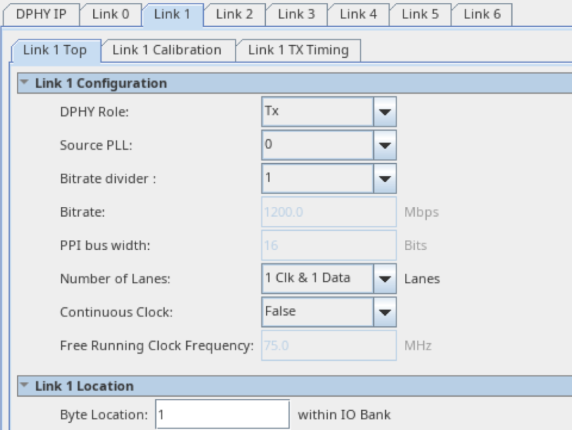
| Parameter Name | Description | Setting |
|---|---|---|
| D-PHY Role | Configure D-PHY mode as Tx or Rx. | Unused, TX, or RX. (Default is Unused.) |
| Source PLL | Specify which PLL source will drive the link's clock. | 0 or 1. (Default value is 0.) |
| Bit Rate Divider | Bit rate divider to keep VCO > 600MHz. Used to divide the TX bit rate. | 1, 2, 4, or 8. (Default value is 8.) |
| Bit Rate | Not available for Tx mode. | D-Series: 150Mbps - 3500Mbps E-Series device group A: 150Mbps - 3500Mbps E-Series device group B: 150Mbps - 2500Mbps |
| PPI bus width | Not available for Tx mode. | 16. |
| Number of Lanes | Set number of data lanes for the link : 1, 2, 4 or 8. | 1 Data & 1 Clk 2 Data & 1 Clk 4 Data & 1 Clk 8 Data & 1 Clk (Default is 1 Data & 1 Clk.) |
| Continuous clock | Specify that the clock lane is continuous. | True or False. (Default value is False.) |
| Free Running Clock Frequency | Not available for Tx mode. | |
| Byte location | Specifies D-PHY links BYTE location within the I/O bank. | 0-7. |
Link Calibration Configuration
On the Link Calibration tab you can enable the skew, alternate, and periodic calibration functions, preamble and TX equalization mode to meet your performance requirements. You can run simulation to validate which TX equalization mode suits your design intent. For data rates above 2.0G, you should set the TX equalization mode to MED LP on Quartus® Prime Pro Edition software version 24.2; if you are using version 24.1, select mode 1.
Figure 15. Link Calibration Tab
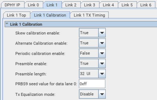
| Parameter Name | Description | Setting |
|---|---|---|
| Skew Calibration Enable | Generate logic to support skew calibration. | True or False. (Default value is False.) |
| Alternate Calibration Enable | Generate logic to support alternate calibration (Show when skew calibration enabled). | True or False. (Default value is False.) |
| Periodic calibration enable | Generate logic to support periodic skew calibration (Show when skew calibration enabled). | True or False. (Default value is False.) |
| Preamble Enabled | Generate logic to support preamble. | True or False. (Default value is False.) |
| Preamble Length | Preamble length settings (when Preamble is enabled). | 32,64,96,128,160,192,224,256,288,320,352,384,416,448,480,512 UI. (Default value is 32.) |
| PRBS9 seed value for data lane n | PRBS value for data lane used by Tx / Rx alt cal and test mode. (Available when Alternate Calibration is enabled.) | 0xFF |
| Tx equalization mode | Tx Equalization mode. | Disable or MED LP or HI LP or MED CZ. (Default value is Disable.) |
Link TX Timing Parameters
On the Link TX Timing tab you can configure the transmit timing parameters..
Figure 16. Link TX Timing Tab
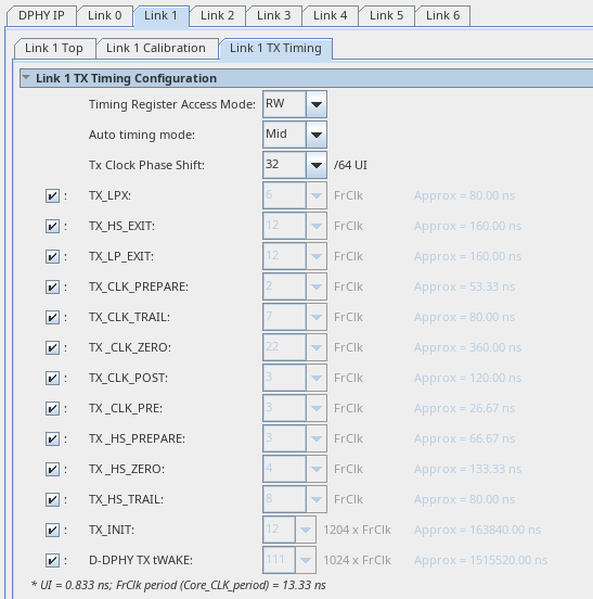
| Parameter Name | Description | Setting |
|---|---|---|
| Timing Register Access Mode | Set to implement timing registers as R/W or RO. R/W register will use up more FPGA resources. | RW or RO. (Default value is RW.) |
| Auto Timing mode | Choose to use min timing, max timing or mid for default values of timing registers set to "Auto". All timing registers have a min specified timing, but not all have a max specified timing. For those with no max specified timing, max Is set to register max value. | Max or Mid or Min. (Default value is Mid.) |
| TX Clock Phase Shift | Sets the phase shift of the clock lane relative to the data lanes. 1 UI is equivalent to 64 steps. Default is 32, shifting clock by 1/2 UI. | 0-63. (Default value is 32.) |
| TX_LPX | Transmitted length of any Low-Power state period. TLPX is an internal PHY timing parameter. TCLK-PREPARE is an external parameter, which can differ from TLPX. | 0-128. (Default value is 6.) |
| TX_HS_Exit | Time that the transmitter drives LP-11 following a HS burst. | 0-255. (Default value is 12.) |
| TX_LP_Exit | Time that the transmitter drives LP-11 between any LP sequences, or between an LP sequence and a HS burst. | 0-255. (Default value is 12.) |
| Tx_CLK_Prepare | Time that the transmitter drives the Clock Lane LP-00 Line state immediately before the HS-0 Line state starting the HS transmission. Delay computation (approx): TCLK-PREPARE = (TX_CLK_PREPARE + 2) * Core_CLK_period. | 0-63. (Default value is 2.) |
| Tx_Clk_Trail | Time that the transmitter drives the HS-0 state after the last payload clock bit of a HS transmission burst. Delay computation (approx): TCLK-TRAIL = (TX_CLK_TRAIL - TXFIFO_LAT) * Core_CLK_period where TXFIFO_LAT might be different for PPI = 16 and 8. | 0-127. (Default value is 7.) |
| Tx_clk_zero | Time that the transmitter drives the HS-0 state prior to starting the Clock. Delay computation (approx): (+ TXFIFO_LAT is intended) TCLK-ZERO = (TX_CLK_ZERO + 2 + TXFIFO_LAT) * Core_CLK_period. | 0-127. (Default value is 22.) |
| Tx_clk_Post | Time that the transmitter continues to send HS clock after the last associated Data Lane has transitioned to LP mode. Interval is defined as the period from the end of THS-TRAIL to the beginning of TCLK-TRAIL. Delay computation (approx) : (+ TXFIFO_LAT is intended) TCLK-POST = (TX_CLK_POST + 2 + TXFIFO_LAT - (2*TX_VCO_FREQ_MULT)) * Core_CLK_period. TX_VCO_FREQ_MULT is the Bit Rate Divider value described on table 14 to target Low Bit Rate speeds on our RX IP. | 0-255. (Default value is 3.) |
| Tx_CLK_Pre | Time that the HS clock shall be driven by the transmitter prior to any associated Data Lane beginning the transition from LP to HS mode. Delay computation: TCLK-PRE = (TX_CLK_PRE + 2 - TXFIFO_LAT) * Core_CLK_period Aligned to data lanes' next ESC clock edge. | 0-15. (Default value is 3.) |
| Tx_HS_Prepare | Time that the transmitter drives the Data Lane LP-00 Line state immediately before the HS-0 Line state starting the HS transmission. Delay computation (approx): THS-PREPARE = (TX_HS_PREPARE + 2) * Core_CLK_period. | 0-63. (Default value is 3.) |
| Tx_HS_Zero | Time that the transmitter drives the HS-0 state prior to transmitting the Sync sequence. Delay computation (approx): (+ TXFIFO_LAT is intended) THS-ZERO = (TX_HS_ZERO + 4 + TXFIFO_LAT ) * Core_CLK_period. | 0-255. (Default value is 4.) |
| Tx_HS_Trail | Time that the transmitter drives the flipped differential state after last payload data bit of a HS transmission burst. Delay computation (approx): THS-TRAIL = (TX_HS_TRAIL + 1 - TXFIFO_LAT - (TX_VCO_FREQ_MULT > 2 ? 8 : 2) ) * CORE_CLK_period. TX_VCO_FREQ_MULT is the Bit Rate Divider value described on table 14 to target Low Bit Rate speeds on our RX IP. | 0-255. (Default value is 8.) |
| Tx_Init | Time that Slave side PHY shall be initialized when the Master PHY drives a Stop State. | 0-255. (Default value is 12.) |
| D-PHY Tx Twake | Time that a transmitter drives a Mark-1 state prior to a Stop state in order to initiate an exit from ULPS. | 0-255. (Default value is 111.) |