Visible to Intel only — GUID: prf1693106337020
Ixiasoft
Visible to Intel only — GUID: prf1693106337020
Ixiasoft
7.6.8.2. Routing Guidelines for DDR5 Memory Down: Single Rank or Dual Rank (x8 bit or x16 bit) Configurations
For example, the maximum length of the main trace routing can be derived from total trace length by subtracting the break-out and break-in trace segment lengths routed.
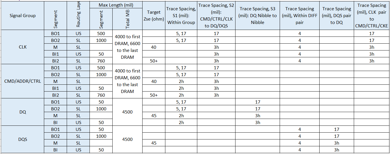
The following table shows physical trace segment routing guidelines, including the target impedance of routing for each signal and the minimum space between signal traces on the same layer. The PCB designer must meet the impedance target criteria. The h in the table indicates the minimum substrate height from signal layer to reference layer. Ensure that you follow the trace-to-trace-edge gap/space criteria in the guideline, based on h in various stackups.

|
Reset signal routing also follows the CMD/ADD/CTRL routing design. Maintain an edge-to-edge space between the Reset signal and other signals on the same layer of at least 3x h. There is no requirement to have skew matching between the Reset signal and CLK signal. Altera recommends using a 1K-ohm pull-down resistor for Reset signal termination, as illustrated below.

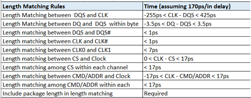
The following table provides a detailed skew matching guideline. Ensure that you include both PCB physical routing skew and package routing skew in your skew matching criteria. The physical length matching criteria in the table reflects the default stackup in our platform PCB design.

|
Board thickness in the design can vary from thin to thick. In this design guideline, a standard thin board is 65 mils and 120 mils thickness is a standard thick board. You can perform simulation to determine whether to use back drill.
| Memory Interface | DDR5 | |
|---|---|---|
| Signal Group | DQ | |
| Board Thickness (mil) | 65 mil or 120 mil (Data Routing must be on upper layers to avoid long via/vertical Xtalk) | 65 mil or 120 mil (Data Routing must be on upper layers to avoid long via/vertical Xtalk) |
| PCB Stripline Trace Impedance (ohms) | 45 | 45 |
| Memory Configuration | Memory Down | Memory Down |
| # of Rank | 1 (40bits total), x8 or x16 | 2 (40 bits total), x8 or x16 |
| Maximum PCB Length Total (inches) to the DRAM | 4.5 | 4.5 |
| Note | Maximum package length in FPGA design is shorter than 34mm | |