Visible to Intel only — GUID: yvn1693244364150
Ixiasoft
Visible to Intel only — GUID: yvn1693244364150
Ixiasoft
8.5.2. General Design Considerations
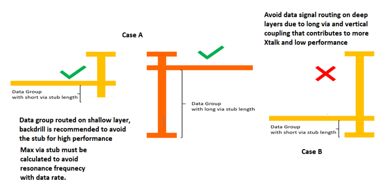
The following figure illustrates a routing example for a Type-III PCB for an LPDDR5 design. Altera recommends that you route Data Group signals such as DQ, DM and DQS on shallow layers as stripline, with the least Z-height via transition to avoid vertical crosstalk for high performance.
Minimal stub effect or back drill is recommended but not mandatory to avoid high reflection for maximum data rate performance for an LPDDR5 interface. You can perform simulation to determine whether to use backdrill. Long via stubs will affect the intersymbol interference (ISI) of the channel, but the impact of ISI is less than the impact of crosstalk for maximum performance.

In the above figure, case A routing is suggested for LPDDR5 Data Group signals over case B, to support maximum data rate. If data signals are routed on deeper layers (as in case B, with long via and short stub), the impact of crosstalk is significant and causes reduced data rate and performance.
To minimize horizontal crosstalk between signals on the same layer, PCB designers must maintain adequate signal trace-to-trace (edge to edge) space with a minimum spacing of 3 x h separation distance, where h is the dielectric thickness to the closest reference plane, as illustrated below. Refer to the routing guidelines sections for detailed spacing requirements for each signal group.
