Visible to Intel only — GUID: hdj1668783688432
Ixiasoft
Visible to Intel only — GUID: hdj1668783688432
Ixiasoft
8.4.1.2. LPDDR5 Component Options
| Pins | 1CH x32 | 2CH x16 | |
|---|---|---|---|
| Data | 32-bit DQ[15:0]_A DQ[15:0]_B |
DQ[15:0]_A |
DQ[15:0]_B |
| Data mask | DM[1:0]_A DM[1:0]_B |
DM[1:0]_A |
DM[1:0]_B |
| Read data strobe | RDQS[1:0]_t_A RDQS[1:0]_c_A RDQS[1:0]_t_B RDQS[1:0]_t_B |
RDQS[1:0]_t_A RDQS[1:0]_c_A |
RDQS[1:0]_t_B RDQS[1:0]_c_B |
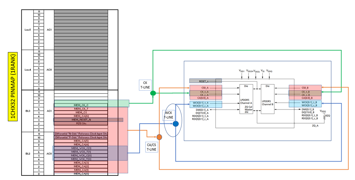
| Write clock | WCK[1:0]_t_A WCK[1:0]_c_A WCK[1:0]_t_B WCK[1:0]_c_B |
WCK[1:0]_t_A WCK[1:0]_c_A |
WCK[1:0]_t_B WCK[1:0]_c_B |
| Command/address | CA[6:0]_A CS0_A CA[6:0]_B CS0_B |
CA[6:0]_A CS0_A |
CA[6:0]_B CS0_B |
| Clock | CK_t_A CK_c_A CK_t_B CK_c_B |
CK_t_A CK_c_A |
CK_t_B CK_c_B |
| Reset | RESET_n |
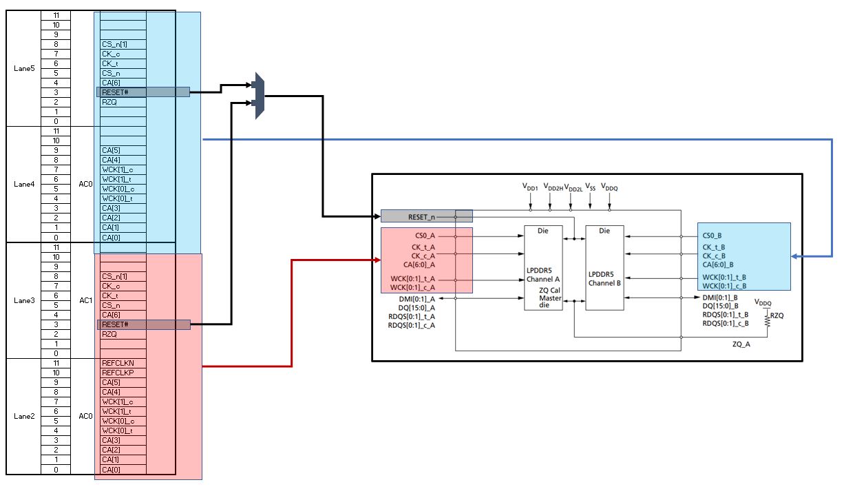
RESET_n (Resistor jumper to select from mem_0 or mem_1.)
Note:
The LPDDR5 EMIF IP design would generate one reset pin to the memory module for both single channel x16/x32 or dual channel x16 design. For early board bring up and easy debugging on dual channel x16 designs, you can test each channel independently as single channel design. You can design the board with two reset pins connected through a resistor jumper to choose the reset from the primary channel or secondary channel. The example for dual channel x16 LPDDR5 with two reset pins is shown in the figure below. For mature designs, you can design the board with one reset pin connected out from the primary channel. |
|

