Visible to Intel only — GUID: skp1693244524683
Ixiasoft
Visible to Intel only — GUID: skp1693244524683
Ixiasoft
8.5.7.1. LPDDR5 Discrete Component/Memory Down Topology, Single Rank or Dual Rank
There are four DRAM interface signal groupings: Data Group, Command-Address Group, Control Group, and Clock Group. The connection between the FPGA and DRAM uses point-to-point topology for Data, Command/Address, Control, and Clocks, as shown in the following figure.

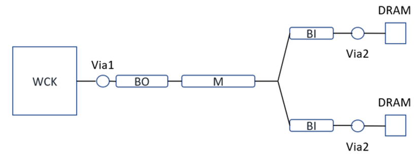
The LPDDR5 interface does not support a traditional dual-directional data-strobe architecture. However, two single-directional data strobes such as Write Clock (WCK) for Write Operations and an optional Read Clock (RDQS) for Read Operations are supported.
The following two figures show the connection topology for DQ, WCK signal and CA, CLK, CTRL signals for LPDDR5.

