Visible to Intel only — GUID: luy1693244616234
Ixiasoft
Visible to Intel only — GUID: luy1693244616234
Ixiasoft
8.5.7.3. Example of an LPDDR5 Layout on an Altera® FPGA Platform Board
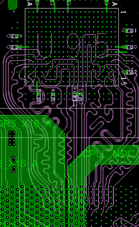
The LPDDR5 signal routing is on upper layers to avoid vertical crosstalk on interface and achieve high performance.


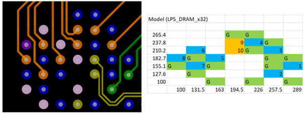
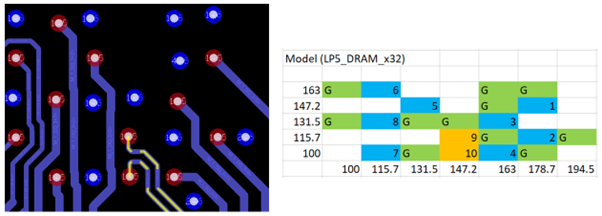
In addition, the following figure shows a LPDDR5 64-bit device board routing sample with pitch dimension of 0.4×0.4mm. The microvia has been used for via transitions on this interface. The microvia mentioned in the following is from top layer to layer 3, it belongs to Type-III stack-up for easier fan-out, not the same as microvia used in Type-IV stack-up. Only one lamination cycle is required, therefore the cost is not increased as much as microvias in Type-IV. You can also use normal PTH with backdrilling to fan out.
