Visible to Intel only — GUID: wlc1693102784891
Ixiasoft
Visible to Intel only — GUID: wlc1693102784891
Ixiasoft
7.6.3. DDR Differential Signals Routing
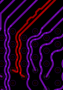
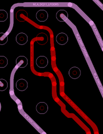
You should have a symmetrical fan-out routing at the FPGA pin field. Non-symmetrical routing for differential signals causes shifting on common-mode voltage and contributes to reduced timing margins at the receiver. The following figures show the recommended differential routing at the FPGA pin field for DQS/CLK signals.


Altera recommends implementing length and skew matching for differential signals immediately after the FPGA device to avoid additional shifting on differential signals common mode voltage.
In cases where very small DRAM device pitch limits the implementation of symmetrical routing at the DRAM pin field for differential signals, it is recommended to route the differential signals as single-ended signals within the DRAM pin field, ensuring to maintain the same impedance while changing from differential to single-ended configuration. Designers must also keep the same length of routing for each P and N single-ended lane within the DRAM pin field. The skew matching between P and N lanes must be applied before reaching the DRAM pin field.