Visible to Intel only — GUID: ohu1498252139806
Ixiasoft
1. Introduction
2. Quick Start Guide
3. Interface Overview
4. Parameters
5. Designing with the IP Core
6. Block Descriptions
7. Registers
8. Programming Model for the DMA Descriptor Controller
9. Programming Model for the Avalon® -MM Root Port
10. Avalon-MM Testbench and Design Example
11. Document Revision History
A. PCI Express Core Architecture
B. Root Port Enumeration
C. Troubleshooting and Observing the Link Status
2.1. Design Components
2.2. Hardware and Software Requirements
2.3. Directory Structure
2.4. Generating the Design Example
2.5. Simulating the Design Example
2.6. Compiling the Design Example and Programming the Device
2.7. Installing the Linux Kernel Driver
2.8. Running the Design Example Application
7.1.1. Register Access Definitions
7.1.2. PCI Configuration Header Registers
7.1.3. PCI Express Capability Structures
7.1.4. Intel Defined VSEC Capability Header
7.1.5. Uncorrectable Internal Error Status Register
7.1.6. Uncorrectable Internal Error Mask Register
7.1.7. Correctable Internal Error Status Register
7.1.8. Correctable Internal Error Mask Register
7.2.1.1. Avalon-MM to PCI Express Interrupt Status Registers
7.2.1.2. Avalon-MM to PCI Express Interrupt Enable Registers
7.2.1.3. Address Mapping for High-Performance Avalon-MM 32-Bit Slave Modules
7.2.1.4. PCI Express to Avalon-MM Interrupt Status and Enable Registers for Endpoints
7.2.1.5. PCI Express Configuration Information Registers
10.5.1. ebfm_barwr Procedure
10.5.2. ebfm_barwr_imm Procedure
10.5.3. ebfm_barrd_wait Procedure
10.5.4. ebfm_barrd_nowt Procedure
10.5.5. ebfm_cfgwr_imm_wait Procedure
10.5.6. ebfm_cfgwr_imm_nowt Procedure
10.5.7. ebfm_cfgrd_wait Procedure
10.5.8. ebfm_cfgrd_nowt Procedure
10.5.9. BFM Configuration Procedures
10.5.10. BFM Shared Memory Access Procedures
10.5.11. BFM Log and Message Procedures
10.5.12. Verilog HDL Formatting Functions
Visible to Intel only — GUID: ohu1498252139806
Ixiasoft
2.5. Simulating the Design Example
Figure 17. Procedure
- Change to the testbench simulation directory, pcie_example_design_tb.
- Run the simulation script for the simulator of your choice. Refer to the table below.
- Analyze the results.
| Simulator | Working Directory | Instructions |
|---|---|---|
| Questa Intel FPGA Edition | <example_design>/pcie_example_design_tb/pcie_example_design_tb/sim/mentor/ |
|
| ModelSim* | <example_design>/pcie_example_design_tb/pcie_example_design_tb/sim/mentor/ |
|
| VCS* | <example_design>/pcie_example_design_tb/pcie_example_design_tb/sim/synopsys/vcs |
|
| NCSim* | <example_design>/pcie_example_design_tb/pcie_example_design_tb/sim/cadence |
|
| Xcelium* Parallel Simulator | <example_design>/pcie_example_design_tb/pcie_example_design_tb/sim/xcelium |
|
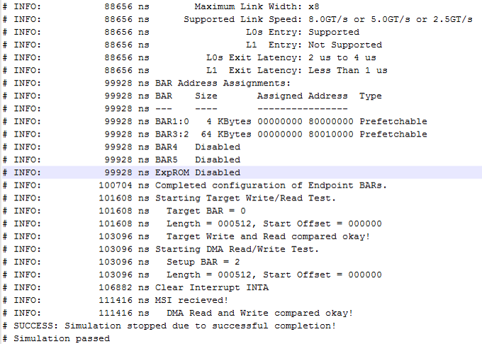
The DMA testbench completes the following tasks:
- Writes to the Endpoint memory using the DUT Endpoint non-bursting Avalon® -MM master interface.
- Reads from Endpoint memory using the DUT Endpoint non-bursting Avalon® -MM master interface.
- Verifies the data using the shmem_chk_ok task.
- Writes to the Endpoint DMA controller, instructing the DMA controller to perform a MRd request to the PCIe* address space in host memory.
- Writes to the Endpoint DMA controller, instructing the DMA controller to perform a MWr request to PCIe* address space in host memory. This MWr uses the data from the previous MRd.
- Verifies the data using the shmem_chk_ok task.
The simulation reports, "Simulation stopped due to successful completion" if no errors occur.
Figure 18. Partial Transcript from Successful Simulation Testbench

