Visible to Intel only — GUID: joc1463007880809
Ixiasoft
Intel® Stratix® 10 Devices and Transceiver Channels
PCB Stackup Selection Guideline
Recommendations for High Speed Signal PCB Routing
FPGA Fan-out Region Design
CFP2/CFP4 Connector Board Layout Design Guideline
QSFP+/zSFP/QSFP28 Connector Board Layout Design Guideline
SMA 2.4-mm Layout Design Guideline
Tyco/Amphenol Interlaken Connector Design Guideline
Electrical Specifications
Document Revision History for AN 766: Intel® Stratix® 10 Devices, High Speed Signal Interface Layout Design Guideline
Option 1: Via-In-Pad Topology
Option 2: Dog-bone with GND Cutout at BGA Pad Topology
Option 3: Micro-via Topology
GND Cutout Under BGA Pads in Fan-out Configuration
Comparison of Dog-bone with GND Cutout Under the BGA and Via-in-Pad Configurations
Trace Shape Routing at the BGA Void Area (Tear Drop Configuration)
Visible to Intel only — GUID: joc1463007880809
Ixiasoft
Option 3: Micro-via Topology
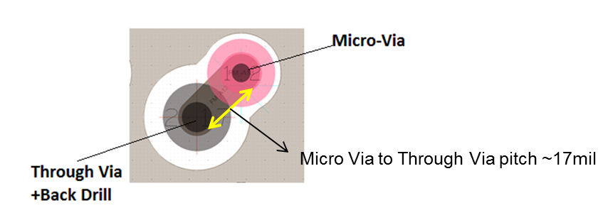
Intel recommends this topology if you use a micro-via technology.
Figure 6. FPGA Fan-out Configuration at Solder Ball for Each Single-ended Lane


Topology specifications:
- Use of “Micro-Via or laser drilled-via” in combination with “Via-in-pad”. Micro-via on FPGA Pad transfers the signal from top layer to the signal pad on the first GND reference layer underneath of top layer. Through via is then used to transit the signal to other layers.
- Micro-via dimensions:
- Via hold/drill diameter: 5 mil
- Via pad diameter: 10 mil
- Via anti-pad diameter: 22 mil
- Through-via dimensions:
- Via hold/drill diameter: 10 mil
- Via pad diameter: 20 mil
- Via anti-pad diameter: 30 mil
- Use of 47.5 Ω single ended trace impedance connecting the micro via pad to Through-via pad on GND reference plane. This 47.5 Ω single ended impedance design is due to match with the targeted 95 Ω differential impedance characteristics design as recommendation for high speed signals routing on PCB. Refer to GND Cutout Under BGA Pads in Fan-out Configuration.
Related Information