AN 766: Intel® Stratix® 10 Devices, High Speed Signal Interface Layout Design Guideline
Visible to Intel only — GUID: joc1463076447125
Ixiasoft
Visible to Intel only — GUID: joc1463076447125
Ixiasoft
FPGA Fan-out Region Routing Recommendations
Intel recommends that you use a 95 Ω differential trace lane for both PCB and fan-out region routing. The tolerance of trace impedance can be within ±10% on the PCB.
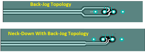
The back-jog routing configuration is best for high speed signals. The advantage of the back-jog configuration is that it keeps the skew matching for both differential lanes in the break out region. Back-jog routing can be either single-ended back-jog or neck-down with back-jog in the fan-out region.

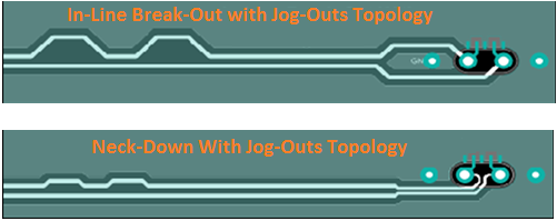
Simulations and measurements show that a traditional jog-out routing configuration in the break-out region degrades performance, specifically for return loss. The traditional jog-out routing requires skew-matching right at the device edge.

For signal data rates above 15 Gbps, Intel recommends that you use a back-jog break-out routing configuration. For data rates lower than 15 Gbps, you must use the jog-out break-out routing with skew matching at the device edge.
For both of these options, single ended routing in the fan-out region results in better insertion loss performance.
Observe these guidelines when routing in the fan-out region:
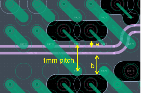
- Route one signal pair between 1 mm BGA pitch for maximum isolation between pairs.
- Keep the fan-out routing length less than 1 inch.
- Avoid routing lanes which are close to the edge of the void area. Maintain enough space between the trace edge and the void edge. A wide reference plane is always required for any high speed signal routing.
