A newer version of this document is available. Customers should click here to go to the newest version.
3.3.1. Project Creation
3.3.2. Design Entry
3.3.3. IP Status
3.3.4. Design Constraints
3.3.5. Synthesis
3.3.6. Design Implementation
3.3.7. Finalize Pinout
3.3.8. Viewing and Editing Design Placement
3.3.9. Static Timing Analysis
3.3.10. Generation of Device Programming Files
3.3.11. Power Analysis
3.3.12. Simulation
3.3.13. Hardware Verification
3.3.14. View Netlist
3.3.15. Design Optimization
3.3.16. Techniques to Improve Productivity
3.3.17. Cross-Probing in the Intel® Quartus® Prime Pro Edition Software
4.2.1.2.1. Memory Mode
4.2.1.2.2. Clocking Mode
4.2.1.2.3. Write and Read Operation Triggering
4.2.1.2.4. Read-During-Write Operation at the Same Address
4.2.1.2.5. Error Correction Code (ECC)
4.2.1.2.6. Byte Enable
4.2.1.2.7. Address Clock Enable
4.2.1.2.8. Parity Bit Support
4.2.1.2.9. Memory Initialization
4.2.1.2.10. Output Synchronous Set/Reset
3.3.2.2. Schematic/Block Editor
In the Intel® Quartus® Prime Pro Edition software, you can use Intel® FPGA-supplied design elements, such as Boolean gates and registers, or you can create your own symbols from HDL or EDA netlist design entities.
- To create a block design file from a VHDL or Verilog HDL design file, click File > Create/Update, and click Create Symbol Files for Current File.
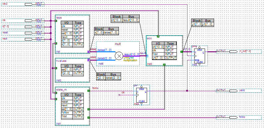
- To create a new schematic file (*.bdf) in the Intel® Quartus® Prime Pro Edition software, point to File > New and select the Block Diagram/Schematic File.
- To insert block symbols into the schematic, double-click the schematic file and choose the appropriate block symbols.
Figure 3. Schematic File

