Visible to Intel only — GUID: xvu1520633284604
Ixiasoft
1. Introduction
2. Quick Start Guide
3. Block and Interface Descriptions
4. Parameters
5. Designing with the IP Core
6. Registers
7. Design Example and Testbench
8. Document Revision History for Intel® L- and H-tile Avalon® Memory-mapped+ IP for PCI Express* User Guide
A. Avalon-MM IP Variants Comparison
B. Root Port BFM
C. BFM Procedures and Functions
D. Troubleshooting and Observing the Link Status
E. Root Port Enumeration
2.1. Design Components
2.2. Directory Structure
2.3. Generating the Design Example
2.4. Simulating the Design Example
2.5. Compiling the Design Example and Programming the Device
2.6. Installing the Linux Kernel Driver
2.7. Running the Design Example Application
2.8. Ensuring the Design Example Meets Timing Requirements
6.1.1. Register Access Definitions
6.1.2. PCI Configuration Header Registers
6.1.3. PCI Express Capability Structures
6.1.4. Intel Defined VSEC Capability Header
6.1.5. Uncorrectable Internal Error Status Register
6.1.6. Uncorrectable Internal Error Mask Register
6.1.7. Correctable Internal Error Status Register
6.1.8. Correctable Internal Error Mask Register
C.1. ebfm_barwr Procedure
C.2. ebfm_barwr_imm Procedure
C.3. ebfm_barrd_wait Procedure
C.4. ebfm_barrd_nowt Procedure
C.5. ebfm_cfgwr_imm_wait Procedure
C.6. ebfm_cfgwr_imm_nowt Procedure
C.7. ebfm_cfgrd_wait Procedure
C.8. ebfm_cfgrd_nowt Procedure
C.9. BFM Configuration Procedures
C.10. BFM Shared Memory Access Procedures
C.11. BFM Log and Message Procedures
C.12. Verilog HDL Formatting Functions
Visible to Intel only — GUID: xvu1520633284604
Ixiasoft
2.4. Simulating the Design Example
Figure 8. Procedure
- Change to the testbench simulation directory, pcie_example_design_tb.
- Run the simulation script for the simulator of your choice. Refer to the table below.
- Analyze the results.
| Simulator | Working Directory | Instructions |
|---|---|---|
| Questa Intel FPGA Edition | <example_design>/pcie_example_design_tb/pcie_example_design_tb/sim/mentor/ |
|
| ModelSim* | <example_design>/pcie_example_design_tb/pcie_example_design_tb/sim/mentor/ |
|
| VCS* | <example_design>/pcie_example_design_tb/pcie_example_design_tb/sim/synopsys/vcs |
|
| NCSim* | <example_design>/pcie_example_design_tb/pcie_example_design_tb/sim/cadence |
|
| Xcelium* Parallel Simulator | <example_design>/pcie_example_design_tb/pcie_example_design_tb/sim/xcelium |
|
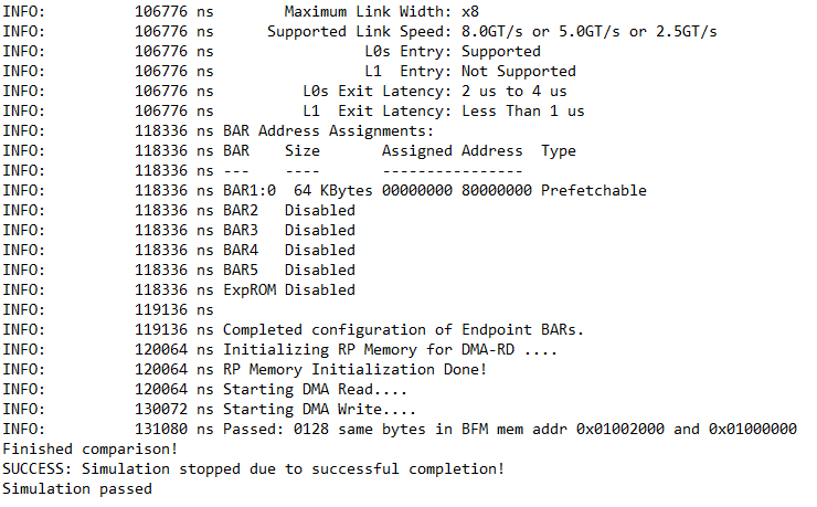
The DMA testbench for the design example completes the following tasks:
- Instructs the Read Data Mover to fetch the descriptors for the DMA Read operation from the PCI Express* system memory.
- The Read Data Mover reads the data from the PCI Express* system memory, and writes the data to the memory in Avalon® -MM address space according to the descriptors fetched in Step 1.
- Instructs the Read Data Mover to fetch the descriptors for the DMA Write operation from the PCI Express* system memory.
- The Write Data Mover reads the data from the memory in the Avalon® -MM address space, and writes the data to the PCI Express* system memory according to the descriptors fetched in Step 3.
- Compares the source data read from system memory in Step 2 to the data written back to the system memory in Step 4.
The simulation reports, "Simulation stopped due to successful completion" if no errors occur.
Figure 9. Partial Transcript from Successful Simulation Testbench

