Visible to Intel only — GUID: nfy1520633344161
Ixiasoft
Visible to Intel only — GUID: nfy1520633344161
Ixiasoft
7.1. Overview of the Example Design
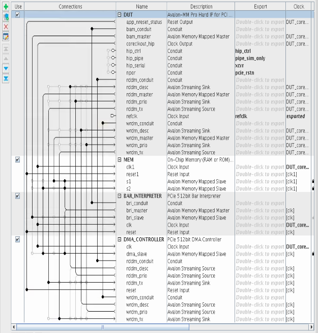
This DMA example design includes a DMA Controller and an on-chip memory to exercise the Data Movers, and a Traffic Generator and Checker to exercise the Bursting Slave.
The example design also connects the Bursting Master to the on-chip memory to allow high-throughput transfers should the host or some other component of the PCIe system be capable of initiating such transfers (e.g. a Root Complex with a DMA engine).
An address translation module is inserted between the Traffic Generator and the Bursting Slave to show an example of how address translation can be performed between the Avalon® and PCIe address spaces.
The on-chip memory that the Data Movers and the Bursting Master connect to is a dual-port memory to allow full-duplex data movement.
The Bursting Master connects to a BAR Interpreter module, which combines the address and BAR number and allows the Bursting Master to control the DMA Controller, the Traffic Generator and the Address Mapper. The BAR Interpreter also connects the Bursting Master to the dual-port memory.
The example design is generated dynamically based on the selected variation of the Intel L-/H-Tile Avalon-MM+ for PCI Express IP. However, some of the user’s parameter selections may need to be overwritten to ensure proper functionality. A warning appears when such a need arises.
The DMA Controller is instantiated for variations that implement at least one of the Data Movers and the Bursting Master. The Traffic Generator and Checker module is instantiated for variations that implement at least the Bursting Slave and the Bursting Master.
You cannot generate an example design for variations that do not implement the Bursting Master as it is necessary for all flavors of the example design. A warning appears to explain that the Bursting Master with appropriate BAR settings must be added in order to generate the example design.
- PIO: This is the variation where only the Bursting Master is enabled. The design example simulation exercises the Bursting Master to perform simple one dword Reads and Writes to the on-chip memory. The BAR Interpreter and on-chip memory are also included in this variation.
- DMA: This is the variation where the Bursting Master, and both of the Read Data Mover and Write Data Mover are enabled. Software sends instructions via the Bursting Master to the Read or Write Data Movers to initiate DMA Reads or Writes to the system memory. The BAR Interpreter, on-chip memory and DMA Controller are also included.
- BAS: This is the variation where the Bursting Master and Bursting Slave are enabled.
- Software writes an instruction via the Bursting Master to the Traffic Generator to generate a block of data, which is then transmitted to the Bursting Slave. Upon receiving the data, the Bursting Slave performs a Memory Write to transfer the data to the PCIe system memory.
- Software then writes another instruction via the Bursting Master to the Traffic Checker, which issues a Read to the Bursting Slave. The Bursting Slave then forms a Memory Read request to fetch the data from the PCIe system memory.
The following figure shows the system-level view in Platform Designer of the DMA example design.
