6.3. Thermal Settings and Parameters
The 1SM21BE device which we are using as the example in this document, is an exception, with a maximum HBM die temperature rating of 95°C. Consequently, for this design we use the Maximum junction temperature mode and set it to 90°C, to provide the design with a margin of 5°C. However, if the analysis indicates that the HBM is not the die with highest temperature, we could then increase the max TJ until the HBM or another die reaches its limit with the margin.
The ambient temperature is set to 50°C.
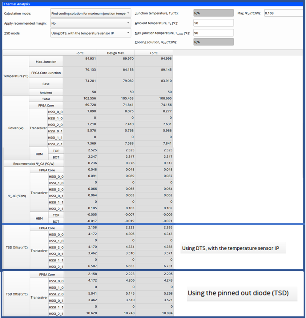
Many designs utilize both sets of sensors, so temperature offset data from both modes is needed. We also assume that our test project uses both sets of thermal sensors. The figure below shows the PTC Thermal page output and the thermal settings and parameters for the design.
The die with the highest ΨJC is the die that has the highest temperature and reaches the maximum TJ for the cooling solution calculated by the PTC. In this case the highest ΨJC of 0.103°C/W belongs to HSS_2_1, E tile transceiver tile. With the maximum TJ set to 90°C, the HBM die has a margin of 5°C, calculating the HBM junction temperature.
TJ_HBM = TCASE + TTP x ΨJC_HBM
TJ_HBM = 79 + 105.453 x -0.007 = 78.26
As expected, the above calculations indicate that the HBM die does not have the highest temperature in this design and the maximum TJ can be increased to 95°C if necessary. Doing so also increases the total power to 108 W and ΨCA to 0.312°C/W from the current 0.276°C/W. The higher the ΨCA value, the easier it is to cool the system; however, the total thermal power (TTP) also increases.
The next step in the process is to contact your Intel Field Application Engineer (FAE) to obtain the compact thermal model (CTM) for the device in the format that you need.