6.7. Heat Sink
For the purpose of this analysis, we are assuming a heat sinks that fits the board and has a vapor chamber base that maximizes thermal conductivity.
Attachment Force
The force with which the heat sink is attached depends on the number of pins in the package and the solder material. For more information about heat sink attachment force, refer to the article What is the maximum downward pressure that can be applied to the top of FPGA BGA packages?.
Thermal Interface Material (TIM)
Intel does not recommend a specific TIM material; however, as a general rule TIMs with higher thermal conductivity perform better. The TIM size is a function of the package interface size to the heat sink, and in the case of our example is about 52x44 mm. Generally, a TIM slightly smaller than the interface size is preferred, to insure better contact; in this example, a TIM of 50x42 mm is recommended. The TIM thickness should not introduce too much resistance, while also ensuring that there is no air pocket between the TIM and the heat sink. In our example, we have chosen a TIM with 0.25 mm thickness and thermal conductivity of 5 W/mk.
CTM Case Temperature Sensor
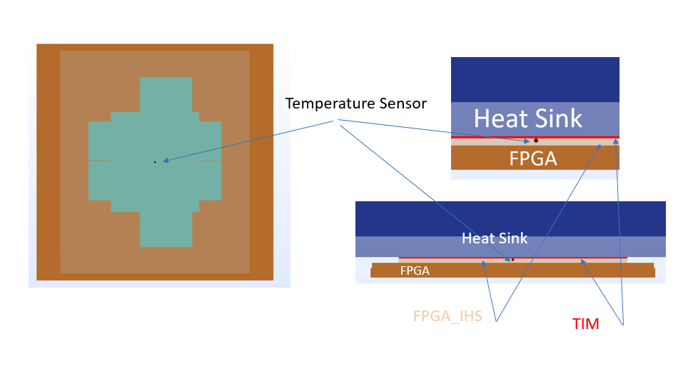
Not all CTMs have a built-in temperature sensor at the center of the integrated heat spreader (IHS). If the CTM for your project does not have a built-in temperature sensor, Intel recommends that you add one. In our example, we have added one. You should place the temperature sensor at the center of the IHS as shown in the figure below. The temperature sensor should not touch the heat sink.
Analysis Settings
For the purpose of this analysis, the airflow at the board inlet boundary is set to 25 CFM at 50°C. The total board power is only the FPGA power at 105 W.
Analysis Results
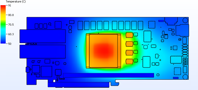
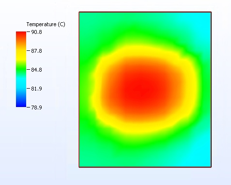
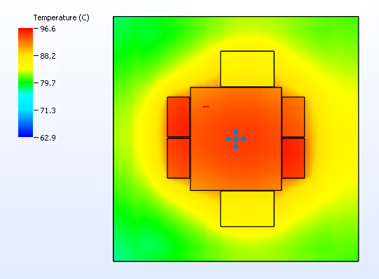
The following figures depict the board, the IHST surface temperature, and the die temperatures from the CFD analysis.
The maximum IHST and core die temperatures are 90.8°C and 95.3°C, respectively. These values are about 10-11°C above the limit of the thermal calculations from the PTC. This indicates that the current cooling solution does not meet the design requirement. If the current cooling solution is implemented, the maximum TJ will be above 90°C and the die powers will be more than what used for this analysis. As stated before, the CFD analysis results are valid only for the core die and the IHS temperatures; the temperature of the transceiver dies are not valid in the CFD analysis
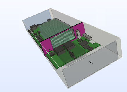
There are several possible methods for improving the cooling; in practice, your thermal/mechanical engineer must make the most appropriate decision. In this example, we will direct air to the heat sink and the DDR memory using a guiding plate, as shown in the figure below.
Using the above solution, the FPGA core and IHST temperatures drop to 80°C and 75.1°C, respectively. These temperature reductions indicate that the cooling system is maintaining the temperatures below the limits of 84°C and 79°C, as recommended by the PTC. The total FPGA power dissipation is now less than what was used in the CFD model, because the lower temperatures reduce the static power consumption.
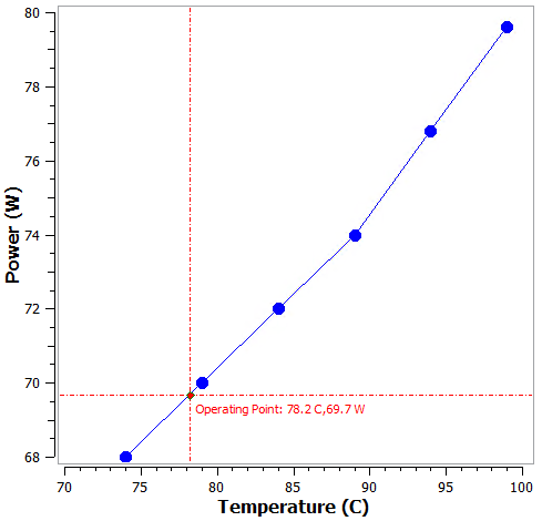
A second run of the PTC with the maximum TJ reduced to 86°C yields a core TJ of 80°C and total power of 103 W. This result is about 2.3 W less than the power used in the current CFD analysis. One method to capture this iteration properly is to enter the core power as a function of temperature. For this, run the PTC with several different maximum TJ settings to obtain the needed powers for the temperature range, and then build the core power curve as a function of its maximum junction temperature. In this case the following curve shows the core die power which we will use in the CFD analysis. For this purpose, we can ignore the static power reduction in the transceiver dies and still use constant power values.
Running the CFD analysis with the new core power setting yields a core die temperature of 78.2°C, which is 2°C less than the previous result. The figure below shows the core power and system operating point. Obviously if the cooling capacity is reduced, the operating point shifts to the right and FPGA total power consumption increases.
