3.7. Planning for an External Memory Interface
This chapter provides details about EMIF IP supported modes, through the hard memory NoC or through NoC bypass, and the latency impact of each mode. Based on your access mode selection, you can encounter differences in supported memory specifications.
This chapter also explains, for each EMIF configuration, the maximum achievable bandwidth, as well as the minimum number of initiators that each configuration requires.
Latency Impact on Different Access Mode shows access to the external memory, regardless of protocol, has the highest latency when accessed through the horizontal NoC. For latency-sensitive applications, use the EMIF in bypass mode to access external memory.
| EMIF in bypass mode (Fabric Sync) | EMIF in bypass mode (Fabric Async) | Via Hard Memory NoC | |
|---|---|---|---|
| Latency Impact | Least | Medium | Most |
Example of Initiators Occupied Per Memory Protocol and Format specifies the number of initiators required, in different memory access modes, across memory format and memory protocols, while using the memory interface in NoC mode. Low latency fabric access (EMIF in bypass mode) blocks some initiators from use. Using the NoC mode does not block initiators.
| Memory Protocol | Memory Format | Total DQ Width | Number of Initiators Required If Using One Initiator Per Channel |
|---|---|---|---|
| DDR4 | Component | x16 | 1 |
| x32 | 1 | ||
| x40(lockstep) | NA | ||
| DIMM | x64(lockstep) | NA | |
| x72(lockstep) | NA | ||
| DDR5 | Component | x16 | 1 |
| 2ch x16 | 2 | ||
| x32 | 1 | ||
| DIMM | 2ch x32 | 2 | |
| LPDDR5 | Component | x16 | 1 |
| 2ch x16 | 2 | ||
| x32 | 1 | ||
| 4ch x16 | 4 |
Example of Initiators Occupied Per Memory Protocol and Format notes:
- DDR4 DIMMs not supported through NoC.
- DDR5 DIMMs contain two channels per DIMM and IP interface.
- LPDDR5 Initiator count is one per channel.
- The choice of I/O bank and associated initiators assumes the existence of only an external memory interface. The choice of initiator may change based on blockages due to HBM2E, LVDS, GPIO, and PHY Lite interfaces, as Example of Initiators Occupied Per Memory Protocol and Format describes.
- The choice of I/O bank and associated initiators assumes a direct connection between the target and initiators.
- Where memory bandwidth is not fully saturated between a target and initiator pair, you can choose to combine multiple initiators to talk to one target, or use fabric NoC to saturate read bandwidth.
As Example of Initiators Occupied Per Memory Protocol and Format shows, NoC mode requires less initiator usage from a per-EMIF-interface perspective. In other words, NoC mode blocks less initiators than bypass mode.
Low latency fabric access blocks initiators. Initiator Blocked Per Memory Protocol and Format specifies the number of initiators blocked in different memory access modes, across memory formats, and memory protocols, while using EMIF in bypass mode.
| Memory Protocol | Memory Format | Total DQ Width | Fabric Async | Fabric Sync | ||
|---|---|---|---|---|---|---|
| IO96B_01 | IO96B_1(5) | IO96B_0(5) | IO96B_1(5) | |||
| DDR4 | Component | x16 | 2 | - | 2 | - |
| x32 | 2 | - | 2 | - | ||
| x40(lockstep) | NA | 3 | - | |||
| DIMM2 | x64(lockstep) | NA | 4 | |||
| x72(lockstep) | NA | 5 | ||||
| DDR5 | Component | x16 | 2 | - | 2 | - |
| 2 x16 | 3 | - | 3 | - | ||
| x32 | 2 | - | 2 | - | ||
| DIMM3 | 2 x32 | 2 | 2 | 2 | 2 | |
| LPDDR5 | Component | x16 | 2 | - | 2 | - |
| 2 x16 | 3 | - | 3 | - | ||
| x32 | 2 | - | 2 | - | ||
| 4 x16 | 3 | 3 | 3 | 3 | ||
You can choose to enable the fabric NoC for your application. Achievable Bandwidth across Memory Protocol and Device Speed Grade highlights the limitations on achievable bandwidth across speed grade, even if external memory runs faster. This impact appears regardless of the hard memory controller and horizontal NoC performance capabilities.
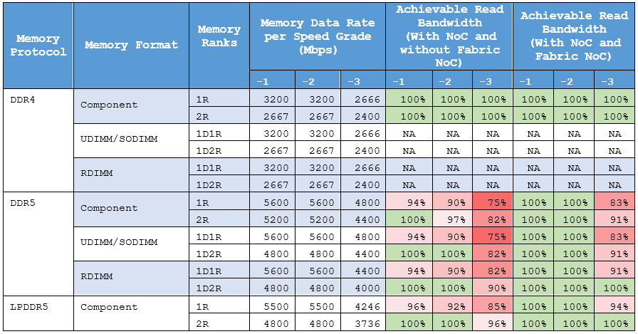
The following notes apply to Achievable Bandwidth across Memory Protocol and Device Speed Grade:
- The table shows achievable bandwidth for memory interface via NoC mode, based on the bandwidth of x32 DQ * (indicated data rate).
- DDR4 DIMM is not supported in the current version of software.
- The achievable bandwidth shown in the table is based on single initiator usage, for a single channel of a given memory protocol, running at the maximum core frequency for each device speed grade.
- Uses green shading to indicate areas with no degradation in bandwidth, and no impact of initiator frequency.
- Uses red shading to indicate the severity of bandwidth loss due to initiator frequency support across different memory access mode.
Based on your application’s bandwidth requirements, consider a memory access mode, either through the NoC or in bypass mode, that can closely meet your application’s expectations. As indicated by the data in Achievable Bandwidth across Memory Protocol and Device Speed Grade, memory access through the NoC with the fabric NoC fully saturates read bandwidth. In situations where initiator bandwidth is not fully saturated between a target and initiator pair, you can choose to combine a single initiator to communicate to multiple targets.
In accordance with the information in this chapter, follow these summary guidelines to achieve latency and bandwidth goals:
- Access external memory interfaces through the NoC to save the number of initiators in latency-insensitive applications.
- To ease bandwidth sharing on horizontal NoC, use the local connection between EMIF targets and initiator, if possible.
- Consider hard memory controller inefficiencies across different access scenarios when determining the bandwidth of external memory access.
- Consider that an application’s cumulative bandwidth highly depends on your controller efficiency, horizontal NoC congestion, and individual initiator’s operating frequency and capacity.
Based on your choice of memory protocol, Intel Agilex 7 M-Series FPGAs supports restrictive pin-outs for various memory formats. For detailed information, refer to External Memory Interfaces Intel Agilex 7 M-Series FPGA IP User Guide.