Visible to Intel only — GUID: mtr1422491951539
Ixiasoft
1. Introduction to Intel® FPGA Design Flow for Xilinx* Users
2. Technology Comparison
3. FPGA Tools Comparison
4. Xilinx* to Intel® FPGA Design Conversion
5. Conclusion
6. AN 307: Intel® FPGA Design Flow for Xilinx* Users Archives
7. Document Revision History for Intel® FPGA Design Flow for Xilinx* Users
3.3.1. Project Creation
3.3.2. Design Entry
3.3.3. IP Status
3.3.4. Design Constraints
3.3.5. Synthesis
3.3.6. Design Implementation
3.3.7. Finalize Pinout
3.3.8. Viewing and Editing Design Placement
3.3.9. Static Timing Analysis
3.3.10. Generation of Device Programming Files
3.3.11. Power Analysis
3.3.12. Simulation
3.3.13. Hardware Verification
3.3.14. View Netlist
3.3.15. Design Optimization
3.3.16. Techniques to Improve Productivity
3.3.17. Partial Reconfiguration
3.3.18. Cross-Probing in the Intel® Quartus® Prime Pro Edition Software
4.2.1.2.1. Memory Mode
4.2.1.2.2. Clocking Mode
4.2.1.2.3. Write and Read Operation Triggering
4.2.1.2.4. Read-During-Write Operation at the Same Address
4.2.1.2.5. Error Correction Code (ECC)
4.2.1.2.6. Byte Enable
4.2.1.2.7. Address Clock Enable
4.2.1.2.8. Parity Bit Support
4.2.1.2.9. Memory Initialization
4.2.1.2.10. Output Synchronous Set/Reset
Visible to Intel only — GUID: mtr1422491951539
Ixiasoft
3.3.7.1. Pin Planner
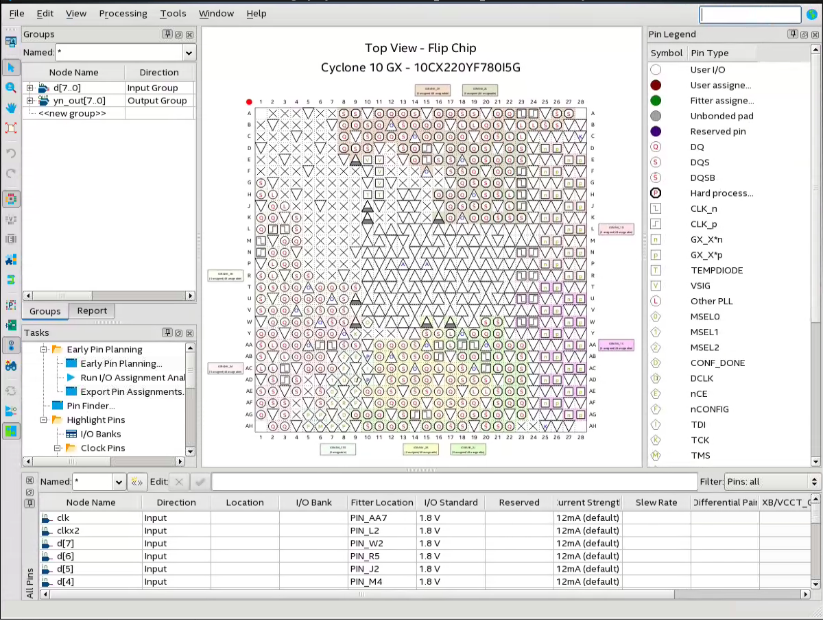
The Intel® Quartus® Prime Pro Edition Pin Planner provides a graphical package view, allowing you to validate I/O assignments by performing legality checks on a design's I/O pins and surrounding logic.
With the Pin Planner, you can identify I/O banks, VREF groups, and differential pin pairings to help you with the I/O planning process. To access the Pin Planner, click Assignments > Pin Planner.
Note: Modifications that you make in the Pin Planner affect the .qsf file.
Figure 7. Intel® Quartus® Prime Pro Edition Pin PlannerTo invoke the Pin Planner, click Assignments > Pin Planner

